3S3P Automotive Rear Light (RCL) LED Driver Reference Design
3S3P Automotive Rear Light (RCL) LED Driver Reference Design
Abstract: This application note describes a reference design for driving a rear light (RCL) LED. The driver uses a three-string three-parallel (3S3P) architecture. The reference design uses the MAX16823 linear driver and an external BJT to provide 200mA drive current for each string of LEDs, improving heat dissipation. The design includes a PWM dimming circuit, which is used to adjust the brightness of the tail light and the full-bright brake light. The design considers dual batteries and load dump.
This reference design uses the MAX16823 3-channel linear LED driver and external BJT to implement the 3S3P RCL drive circuit. Figures 1 and 2 give pictures of the PCB and the heat sink installed; Figure 3 is the circuit board layout of the reference design; Figure 4 is the schematic of the reference design.
The reference design is discussed in detail below, and the analysis, design specifications, and test data of the main functional circuits are given. 
Detailed image (PDF, 1.89MB)
Figure 1. PCB and mounted heat sink 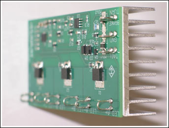
Detailed image (PDF, 1.49MB)
Figure 2. Side view with radiator installed 
Detailed pictures (PDF, 320kB)
Figure 3. LED driver wiring 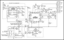
Detailed picture (PDF, 116kB)
Figure 4. Schematic diagram of the LED driver
The reference design consists of four parts of the circuit: input protection circuit and input selector, 10% duty cycle generator, load dump and dual battery detection, LED drive circuit.
Input protection is mainly provided by metal oxide varistor MOV1 and MOV2. In the design, we used Littelfuse's V18MLA1210H (EPCOS also provides high-quality MOV devices). According to the specific application environment, choose MOVs with different rated joules.
After the input voltage is established, the input selector switches the power supply to the tail light node unless a valid power is applied to the brake light / turn signal input. Once the power supply supplies power to the brake light / turn signal input, the input selector will automatically shield the tail lamp input current. This architecture will provide 600mA current for the brake light / turn signal input, indicating the RCL function. When the LED driver fails or the LED itself fails, the MAX16823 will completely turn off all the LEDs. At this time, only less than 5mA of current flows out of the brake lights / turn signals. The output stage circuit of the lamp can successfully detect this low current and issue an alarm signal according to the design requirements.
D5 and R16 make up the detection circuit. When the tail lamp input node voltage is 9V or higher, and the brake lamp / turn signal input node is grounded or high impedance, the detection circuit turns on Q4. The input voltage is loaded to VIN through diode D3, which provides the main power supply for the LED driver. When the input voltage of the brake light / turn signal reaches within 2V of the tail light voltage, Q4 is turned off, and VIN is powered by the diode D4. R17 provides 2.1kΩ resistance to ground to ensure the maximum impedance of this node. The power of R17 reaches 270mW under the condition of dual batteries (24V), so a resistor of 0.5W power must be selected. The main limitation of this circuit is: When the brake lights / turn signals and tail lights work simultaneously, it is assumed that the difference between the input voltages of the brake lights / turn signals and the tail lights is within 2V.
The 10% duty cycle generator generates a square wave signal with a duty cycle of 10%. This signal is sent to the MAX16823 LED driver for adjusting the LED brightness. As long as the tail light input provides an effective voltage, the dimming circuit will work effectively. R10 and D2 provide a 5.1V voltage regulator source for U3 (ICM7555ISA) power supply. Under the dual battery condition, since the power consumption may reach 44mW, R10 must select a resistor with 0.25W power. Timer U3 is configured as an unstable oscillator, the on-time is determined by the time to charge C6 through D1 and R11 (tON = 0.693 × R11 × C6 = 0.418ms [typical]); the off-time is determined by passing R12 to C6 The discharge time is determined (tOFF = 0.693 × R12 × C6 = 3.8ms [typical value]). The sum of on-time and off-time constitutes a square wave signal with a period of approximately 237 Hz, with a duty cycle of 9.9%. Figure 5 shows the duty cycle.
Resistor R13 provides current-limiting protection and reduces the possible EMI radiation generated by the switch node. The physical location of R13 should be as close to U3 as possible to reduce EMI. A square wave signal with a duty cycle of 10% is coupled to U1 through D7 and R14. As long as the brake light / turn signal does not have a valid power supply, the logical OR circuit provided by D7 will allow the 10% duty cycle pulse to pass through. This configuration provides lower LED brightness when the supply voltage is applied to the tail light input. When the brake light / turn signal input effective voltage, D7 provides voltage to DIM1, DIM2 and DIM3 input, so that the LED brightness reaches 100% (high LED brightness). Because the LEDGOOD signal cannot exceed 6V, resistor R14 limits the current to less than 2mA, and D9 and D2 provide voltage clamping to avoid excessively high node voltages. When no voltage is applied to the anode of D7, resistor R15 is a pull-down resistor. When using a 400kΩ resistor, R15 will keep the DIM node voltage below 0.6V, and the current sink at this time is 1.5µA—much lower than the 0.1µA source current of the DIM input. 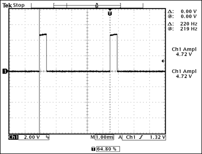
Figure 5. Oscillator output
The load dump and dual battery detection circuit determine whether or not the logic input voltage exceeds 21V. Input voltage exceeding 21V means load dump (400ms) or dual battery condition (no time limit), which will cause excessive power consumption on the three LED drive transistors. Therefore, the detection circuit pulls the DIMx input low and turns off the output driver. In addition, the detection circuit also pulls the LGC capacitor (C2) low to avoid possible erroneous detection. Since the voltages of the DIMx and LGC pins are controlled within 10V, the rated voltages of Q5 and D6 are not strict. The detection voltage is the sum of the breakdown voltage of D8 and the voltage of R18 to ground, which is about 22V. When the resistance is 20kΩ, R9 will generate a bypass leakage current of 20µA before Q5 turns on.
The core IC of the reference design is the MAX16823ATE LED driver, and the input voltage of the IN pin is up to 45V. The IC supplies current from the OUTx pin to drive the LED. Using a current-sense resistor to detect the current, the MAX16823 regulates the output current of the OUTx pin and maintains the voltage at the CS pin at 203mV as needed. Because each output channel of the IC itself can only provide 70mA output, we have added an external drive to each string of LEDs to provide a drive current of 200mA for each string of LEDs, and help solve the heat dissipation problem. Transistors Q1, Q2, and Q3 (ZXT690BKTC) provide the required current gain. These transistors are provided in a TO-262 package to provide good heat dissipation for the die.
Q1, Q2 and Q3 are 45V, 2A transistors and have a saturation voltage drop VCE (Sat) of less than 200mV when the IC / IB gain is 200 times. Because the voltage difference between the minimum input voltage (9V) and the maximum on-voltage of the LED string (3 × 2.65V = 7.95V) is only 1.05V, the VCE (Sat) rating is very important, and sufficient design margin must be left To meet the voltage drop of Q4 and D3, as well as the VCE (Sat) requirements of Q1, Q2 and Q3, please refer to the data sheet for details.
The resistor divider network R1 / R2, R3 / R4 and R5 / R6 ensure that the output current of each OUTx is not less than 5mA, thus ensuring the stable operation of the IC. In the design step, the minimum and maximum values ​​of the transistor base current are analyzed. These currents flow through resistors R1, R3 and R5. The sum of the voltage drop across the resistor, the VBE of the transistor, and the voltage drop across the sense resistor is the voltage across R2, R4, and R6. Choose these resistors reasonably to ensure that the sum of the current flowing through the resistor and the base current of the transistor is not less than 5mA. On the other hand, the output current of OUTx must be less than 70mA (rated current), please refer to the data sheet for details.
In this design, the adjustment tube needs to dissipate 6W of power. In order to reduce the temperature rise of the transistor, the transistor pad is connected to the bottom layer of the PCB through multiple vias, and the heat is transferred through the electrically insulating (but thermally conductive) adhesive pad Onto the aluminum radiator. When the radiator dissipates 6W of power, its temperature rises by 31 ° C. Although Zetex transistors do not give junction-to-case thermal resistance, you can refer to the thermal resistance of TO-262 packages provided by other transistor suppliers, which is about 3.4 ° C / W. This thermal resistance means that the temperature inside each transistor will be 5.4 ° C higher than the case. In short, under the worst operating conditions, the junction temperature is 35 ° C to 40 ° C higher than the ambient temperature. The temperature actually measured by this reference design is approximately 30 ° C higher.
Figures 6 and 7 show the transient response of the transistor when the tail lamp is powered. During the test, the oscillator outputs a 10% duty cycle pulse signal to pulse-width modulate the MAX16823 to drive the external transistor on / off; the undershoot in Figure 6 lasts for 3µs, and the overshoot in Figure 7 lasts for 100µs. any problem. 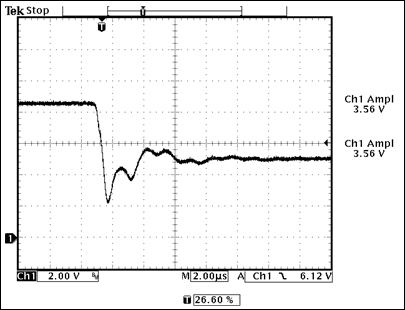
Figure 6. The collector waveform of Q1 when the transistor is on (VIN = 12.5V) 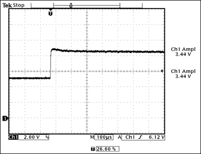
Figure 7. The waveform of the collector of Q1 when the transistor is off (VIN = 12.5V)
Rotor Core,Copper Rotors,Copper Rotors With Shafts,Rotor Assembly
Henan Yongrong Power Co., Ltd , https://www.hnyongrongglobal.com