We often compare the crystal oscillator to the heart of the digital circuit. This is because all the work of the digital circuit is inseparable from the clock signal. The crystal oscillator directly controls the whole system. If the crystal oscillator does not work, the whole system will be paralyzed, so the crystal oscillator is decided. A prerequisite for the digital circuit to start working.
The crystal oscillators we often say are quartz crystal oscillators and quartz crystal resonators. They are all made by the piezoelectric effect of quartz crystals. Applying an electric field to the two electrodes of the quartz crystal causes mechanical deformation of the crystal. Conversely, if mechanical pressure is applied to both sides of the crystal, an electric field is generated on the crystal. And, these two phenomena are reversible. With this characteristic, an alternating voltage is applied to both sides of the crystal, and the wafer generates mechanical vibration while generating an alternating electric field. This type of vibration and electric field is generally small, but at a certain frequency, the amplitude is significantly increased. This is the piezoelectric resonance, similar to the LC loop resonance we often see.
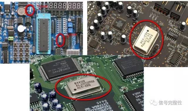
As the heart of digital circuits, how does crystal oscillator work in smart products? For smart homes such as air conditioners, curtains, security, surveillance and other products, wireless transmission modules are required. They send modules from one end to the other through Bluetooth, WIFI or ZIGBEE protocols, or directly through the mobile phone, and the crystal oscillator is The core components in the wireless module affect the stability of the whole system, so choosing the crystal oscillator used by the system determines the success or failure of the digital circuit.
Due to the importance of the crystal oscillator in digital circuits, we need to be careful when using and designing:
1. There is a quartz crystal inside the crystal oscillator. When the external impact or drop occurs, the quartz crystal breaks and breaks, and the crystal oscillator does not vibrate. Therefore, when designing the circuit, consider the reliable installation of the crystal oscillator. The position should be as close as possible to the edge of the board and the device casing. Wait.
2. Pay attention to the welding temperature when welding by hand or machine. The crystal is sensitive to temperature, the temperature during soldering should not be too high, and the heating time should be as short as possible.
Reasonable crystal layout can suppress system radiation interference
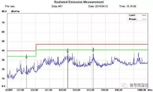
First, the problem descriptionThe product is a field camera, which is divided into five parts: the core control board, the sensor board, the camera, the SD memory card and the battery. The outer casing is a plastic case. The small board has only two interfaces: DC5V external power interface and USB interface for data transmission. Radiation tests have found that there are about 33MHz harmonic noise problems.
The original test data is as follows:
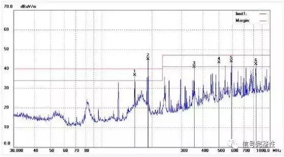
The outer casing of the product is a plastic casing. It is a non-shielded material. The whole machine only tests the power cable and the USB cable to pull out the casing. Is the interference frequency radiated by the power cable and the USB cable? Therefore, I made a few steps to test:
(1) Add a magnetic ring only on the power line, the test result: the improvement is not obvious;
(2) Adding a magnetic ring only on the USB cable, the test result: the improvement is still not obvious;
(3) Add magnetic rings to both the USB cable and the power cable. The test results are: the improvement is obvious, and the interference frequency is reduced overall.
From the above, the interference frequency is brought out from the two interfaces. It is not a problem of the power interface or the USB interface, but the internal interference frequency is coupled to the two interfaces. Only shielding one interface cannot solve the problem. problem.
After near-field measurement, the interference frequency comes from a 32.768KHz crystal oscillator on the core control board, which generates strong spatial radiation, so that the surrounding trace and GND are coupled with 32.768KHz harmonic noise, and then through the interface. The USB cable and the power cable are coupled out to radiate. The problem with this crystal is caused by the following two problems:
(1) The crystal oscillator is too close to the edge of the board, which is likely to cause crystal radiation noise.
(2) There is a cloth signal line under the crystal oscillator, which is easy to cause harmonic noise of the signal line to couple the crystal oscillator.
(3) The filter component is placed under the crystal oscillator, and the filter capacitor and the matching resistor are not arranged according to the signal flow direction, so that the filter effect of the filter component is deteriorated.
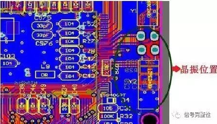
According to the analysis, the following countermeasures are obtained:
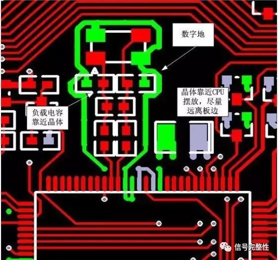
(1) The filter capacitor and matching resistor of the crystal are placed close to the CPU chip, away from the edge of the board;
(2) Remember that the floor cannot be placed in the crystal placement area and the lower projection area;
(3) The filter capacitor and matching resistor of the crystal are arranged according to the flow direction of the signal, and are placed neatly and compactly close to the crystal;
(4) The crystal is placed close to the chip, and the trace between the two is as short and straight as possible.
Can refer to the following layout:
After the rectification, the prototype test results are as follows:
Many system crystal oscillators today have many system crystal clocks with high clock frequency and strong interference harmonic energy. Interfering harmonics are radiated from space except for the two traces of their input and output. If the layout is unreasonable, it is easy to cause strong The problem of noise radiation is difficult to solve by other methods, so it is very important to layout the crystal and CLK signal lines during PCB layout.
Crystal PCB PCB Design Considerations
(1) The coupling capacitor should be placed as close as possible to the power supply pin of the crystal oscillator. The position is placed in the order of the power supply inflow direction. The capacitance values ​​are placed from the largest to the smallest, and the capacitor with the smallest capacitance is closest to the power supply pin.
(2) The outer shell of the crystal must be grounded, radiated outward from the crystal, or shielded from external signals to interfere with the crystal.
(3) Do not route the crystal under the crystal to ensure complete grounding, and do not route the crystal within 300 mil range. This will prevent the crystal from interfering with the performance of other wiring, devices and layers.
(4) The trace of the clock signal should be as short as possible, the line width should be larger, and the balance should be found in the length of the wiring and away from the heat source.
(5) Do not place the crystal on the edge of the PCB. Pay special attention to this point when designing the board.
Ball Grid Array (BGA), a type of surface-mount packaging (a chip carrier) used for integrated circuits.
OEM needs smaller and more diverse packaging options to meet product design challenges and maintain cost competitiveness in their respective markets. Ball grid array (BGA) packaging is becoming more and more popular to meet these design requirements. In addition, they are ideal solutions, because I/O connections are located inside the device, increasing the ratio of pins to PCB area. In addition, BGA with strong solder balls is stronger than QFP lead, so it is more robust.
Ball-Grid Array (BGA) Packages Become PCB Design Mainstream
BGA PCB Design Guidelines And Rules
BGA PCB Design Rules
In order to keep up with the technological progress of chip manufacturers, BGA software packages for embedded design have made remarkable progress in the past few years.
This special type of packaging can be decomposed into standard BGA and micro BGA.
With today's electronics technology, the demand for I/O availability poses a number of challenges, even for experienced PCB designers, due to multiple exit routes.
Correct BGA partitioning first takes into account uniformity of the partitioning, itself. Because, precise BGA partitioning on a PCB is a crucial design aspect to minimize or eliminate crosstalk and noise, as well as manufacturing issues.
Memory signals need special consideration during BGA partitioning. They need to be away from oscillating signals and power supply switching. This is important because memory signals needs to be clean. If traces carrying these signals are in the proximity of oscillating signals or switching power supply signals, they produce ripples in the memory signal traces, thereby reducing system speed. The system is operational, but at less than optimal speed levels.
BGA PCB Design Guidelines
BGA Design Strategy 1: Define an appropriate exit path
The main challenge for PCB designers is to develop appropriate exit routes without causing manufacturing failures or other problems. Several PCBs need to ensure proper fan-out wiring strategies, including pad and pass size, I/O pin number, layers required for fan-out BGA and line width spacing.
BGA Design Strategy 2: Identify the Layers Required
Another question is how many layers the PCB layout should have, which is by no means a simple decision. More layers mean higher overall cost of the product. On the other hand, sometimes you need more layers to suppress the amount of noise PCB may encounter.
Once the alignment and space width of PCB design, the size of through holes and the alignment in a single channel are determined, they can determine the number of layers they need. Best practice is to minimize the use of I/O pins to reduce the number of layers. Usually, the first two outer sides of the device do not need through holes, while the inner part needs to arrange through holes below them.
Many designers call it dog bones. It is a short path of the BGA device pad, with a through-hole at the other end. The dog bone fan comes out and divides the equipment into four parts. This allows the remaining internal padding to be accessed by another layer and provides escape paths away from the edge of the device. This process will continue until all mats are fully developed.

BGA Package Types
There are six different BGA packages.
1. Moulded Array Process Ball Grid Array (MAPBGA): It is a BGA package which provides low inductance and simple surface mounting.
2. Plastic Ball Grid Array (PBGA): Again, this BGA package provides low inductance, simple surface mounting, high reliability and is cheap.
3. Thermally Enhanced Plastic Ball Grid Array (TEPBGA): Just like its name sound, this BGA package can handle great levels of heat dissipation. Its substrate has solid copper planes.
4. Tape Ball Grid Array (TBGA): You can use this BGA package as a solution for medium- to high- end applications.
5. Package on Package (PoP): It will permit you to put a memory device on some base device.
6. Micro BGA: This BGA package is quite small when compared with standard BGA packages. Currently, you will see 0.65, 0.75 and 0.8 mm pitch size dominating in the industry.
BGA PCB Assembly
Previously, Engineers were not sure whether PCB BGA assembly would be able to achieve the reliability level of traditional SMT methods. However, at present, this is no longer a problem, because BGA has been widely used in prototype PCB assembly and mass production PCB assembly.
You will need to use reflow methods to solder a BGA package. Because only reflux method can ensure solder melting under BGA module.
We have a wealth of experience handling all types of BGAs, including DSBGA and other Complex Components, from micro BGAs (2mmX3mm) to large size BGAs (45 mm); from ceramic BGAs to plastic BGAs. We are capable of placing minimum 0.4 mm pitch BGAs on your PCB.
PCB BGA Advantages
With PCB BGA, you will get the following advantages:
1. BGA package eliminates the issue of developing small packages for ICs with lots of pins.
2. Again, when compared with packages with legs, The BGA package has a lower thermal resistance when placed on the PCB.
3. Do you know which property causes unwanted signals distortion in high-speed electronic circuits? The unwanted inductance in an electrical conductor is responsible for this phenomenon. However, BGAs have very little distance between PCB and the package which in turn leads to lower lead inductance. Thus, you will get top-class electrical performance with pinned devices.
4. With BGAs, you can effectively utilize your printed circuit board space.
5. Another advantage that will come with BGA is the reduced thickness of the package.
6. Last but not least, you will get enhanced re-workability because of bigger pad sizes.

Additional Information
Via in PAD(VIP) PCB
6 Layer BGA PCB
Bare PCB,BGA PCB,BGA Circuit Board,BGA PCB Design
JingHongYi PCB (HK) Co., Limited , https://www.pcbjhy.com