The TL494 is a fixed frequency pulse width modulation circuit that includes all the functions required for switching power supply control. It is widely used in bridge single-ended forward double-tube, half-, full-bridge switching power supplies.
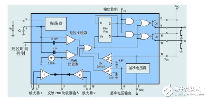
How TL494 worksThe TL494 is a fixed-frequency pulse width modulation circuit with a built-in linear sawtooth oscillator. The oscillation frequency can be adjusted by an external resistor and a capacitor. The oscillation frequency is as follows:

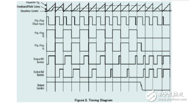
The width of the output pulse is achieved by comparing the positive sawtooth voltage on the capacitor CT with the other two control signals. Power output tubes Q1 and Q2 are controlled by a NOR gate. When the clock signal of the bistable flip-flop is low, it will be strobed, that is, it will be strobed only when the sawtooth voltage is greater than the control signal. As the control signal increases, the width of the output pulse will decrease.
The control signal is input from the outside of the integrated circuit, sent all the way to the dead time comparator, and sent to the input of the error amplifier. The dead time compares the 120mV input compensation voltage, which limits the minimum output dead time to approximately 4% of the sawtooth period. When the output is grounded, the maximum output duty cycle is 96% and the output is connected to the reference level. The space ratio is 48%. When the dead time control input is connected to a fixed voltage (ranging between 0 and 3.3V), an additional dead time can be generated on the input pulse.

The pulse width modulation comparator provides a means for the error amplifier to adjust the output pulse width: when the feedback voltage changes from 0.5V to 3.5, the maximum on-time percentage determined by the pulse width region of the output drops to zero. The two error amplifiers have a common-mode input range from -0.3V to (Vcc-2.0), which may be perceived from the electrical output voltage and current. The output of the error amplifier is always at a high level. It is ORed with the inverting input of the pulse width modulator. The positive circuit structure allows the amplifier to control the control loop with a minimum output.

When the comparator CT discharges, a positive pulse appears at the output of the dead-band comparator, and the pulse-constrained bistable flip-flop counts while stopping the output of Q1 and Q2. If the output control terminal is connected to a reference voltage source, the modulation pulse is alternately output to two output transistors with an output frequency equal to half of the pulse oscillator. If operating in a single-ended state and the maximum duty cycle is less than 50%, the output drive signals are taken from transistor Q1 or Q2, respectively. The output transformer has a feedback winding and a diode that provides a feedback voltage. In single-ended operation mode, when higher drive current output is required, Q1 and Q2 can also be used in parallel. In this case, the output mode control pin should be grounded to turn off the bistable trigger. In this state, the pulse frequency of the input will be equal to the frequency of the oscillator.
Shenzhen Aierbaita Technology Co., Ltd. , https://www.aierbaitavape.com