This design uses ARM processor and embedded operating system μC/OS-II as the development platform in the system terminal. By using ARM processor, the CPU operating frequency can be up to 60MHz, which makes the data processing capability greatly enhanced. At the same time, based on embedding The software developed by the operating system μC/OS-II has strong scalability and stability.
This article refers to the address: http://
system structure
1 Function Introduction The car GPS navigation system obtains the latitude and longitude of the location at that time by the GPS system. The actual position at the time is obtained on the map through conversion and map matching. Then the user inputs the destination and calculates the shortest path through the A* shortest path algorithm. Display on the vector map, and extract the speed, time and other information provided by the GPS and display it on the screen.
2 system Hardware structure The hardware core of the system is the 16/32-bit RISC processor STR710FZ2T6 chip in ARM7 series of STMicroelectronics. The chip has rich peripherals and enhanced I/O functions to meet low power consumption and high performance. Embedded system applications also have an external memory interface (EMI) that can address four memory segments, support multiple memory types such as SRAM, Flash, and ROM, while supporting multiple boot modes. It is very suitable for the development of embedded systems, the system is based on these characteristics of the chip. The system block diagram is shown in Figure 1.
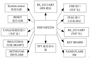
Figure 1 hardware block diagram
The system is based on the STR710FZ2T6 microprocessor and uses two 512KB SDRAMs (IS61LV25616), one 8MB NAND Flash and one 2MB NOR Flash (SST39LF160). A GPS module for receiving GPS signals, a liquid crystal panel for display, and a Keyboard input module are externally added.
1RS-232 serial communication interface circuit In the design of this paper, the system uses RS-232 serial interface for data transmission with the outside world. The circuit is shown in Figure 2. The STR710FZ2T6 has a full-duplex serial communication interface that enables data communication with the GPS module and uses the MAX3232 chip to convert between RS-232 levels and TTL levels.
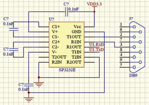
Figure 2 serial communication circuit
SP3232E is an RS232 interface chip produced by Sipex. It is powered by a single Power Supply voltage. The power supply voltage can work normally from 3.0 to 5.5V, and its rated current is 300μA. Only need to externally connect four 0.1μF capacitors to ensure the data transmission rate maintains the RS232 output level at 120Kb/s, which can easily convert between TTL level and RS232 level.
2USB interface circuit In order to develop the USB function, the USB port is set first, and the interface circuit is shown in Figure 3.
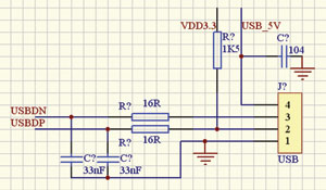
Figure 3 USB interface circuit
3 ARM control module embedded development of the choice of hardware platform is mainly the choice of embedded processor, what embedded processor core used in a system depends mainly on the application domain, user needs, cost, development difficulties Factors such as ease of use. After determining which embedded processor core to use, the next step is to select a suitable processor based on the actual situation and consider the requirements of the system peripherals. In this design, the data processing and control module is the core control component of the vehicle-mounted terminal. It is an embedded system based on ARM microprocessor. Its main function is to process and control the components of the vehicle-mounted terminal, and follow the communication protocol. The requirements to perform the corresponding operations. The system includes CPU memory, I/O interfaces, and various control logic circuits. Combined with the actual situation of the current civilian vehicles, the STR710FZ2T6 microprocessor is selected, which adopts a high-performance 32-bit structure, featuring a high-density 16-bit instruction set and low power consumption, and combines the processor core with on-chip high-speed memory. The peripheral functions of the project are combined on a single microprocessor to provide a flexible, low-cost solution for a large number of computer embedded control applications.
4 The GPS module used in the GPS module system communicates with the microprocessor control module through asynchronous serial communication. Only two signal lines TXD, RXD and ground can be connected to the hardware connection for data transmission.
Serial communication uses a high communication voltage ±5 ~ ± 15V, often using ± 10V and ± 12V, and is a negative logic level, that is, the logic 0 level is specified as +5 ~ +15V, the logic 1 level is specified as - 15 to -5V, so the level conversion must be between the standard serial interface and the TTL/CMOS level.
In the design, the serial communication interface uses Maxim's MAX232 as the conversion chip. The MAX232 can convert two sets of serial signals. In this design, only one set is converted. TXD2 and RXD2 are connected to the peripheral GPS, and MCU_RXD is connected to the MCU_TXD and ARM processors. The four lμF charging capacitors connected to the MAX232 chip can work with an external 5V voltage.
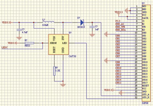
Figure 4 shows the module
5 Display Module This design uses TG160128 liquid crystal display module with direct access. Connect the LCD module of the built-in 6963 controller directly to the P0 and P2 ports of the STR710FZ2T6. The read and write of the display module is controlled by the ARM read and write operation signals. The received and processed navigation information is then output to the Frame Buffer. At this time, the precise longitude, latitude and local time of the positioning point can be displayed on the display screen. The specific circuit is shown in Figure 4.
software design
1 Software data design The data in the navigation software is mainly the spatial data of the navigation map, which is mainly composed of some information related to navigation requirements, including road network geometry, road grade and service facilities. 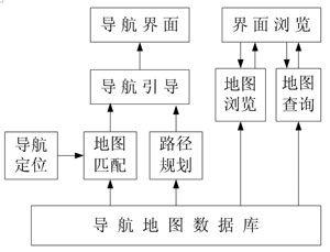
Figure 5 software system block diagram
2 software system design navigation software is based on the navigation database. For the operation behavior of the navigation database, the navigation software is functionally divided into a part with navigation function and a part with browsing function.
3 Software interface design As mentioned above, the navigation software from the large function is divided into a part with browsing function and a part with navigation function. Therefore, two different interfaces have been designed: the browsing interface and the navigation interface.
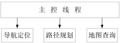
Figure 6 thread diagram
4 embedded software design
The embedded system adopts the μC/OSII operating system. Since the processing function of the MCU is limited, multi-threading technology is adopted in the specific software implementation process, as shown in FIG. 6.
Mario Pcb Board,Mario Bros Pcb Board,Super Mario Bros Pcb Board,Mario Pcb Motherboard
Guangzhou Ruihong Electronic Technology CO.,Ltd , https://www.callegame.com