In the design of single chip microcomputer system, LED display mode has been widely used due to its advantages of convenient use and low price. When the parallel display mode is adopted, the segment code and the bit control code of the display circuit occupy more mouth lines of the single chip microcomputer. Although the interface chip such as 8155 can be used for expansion, the port line utilization rate is still low, which cannot satisfy the requirements of the large control system. Claim. The serial display mode only takes 2 to 3 port lines, which saves a lot of I/O lines of the MCU, and the effect is very good. This task uses the 74HC595A to achieve multi-bit LED serial display.
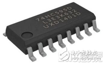
74HC595 chip
1.74HC595A working principle
The 74HC595A contains an 8-bit shift register and an 8-bit D latch. The internal structure is shown in the figure.
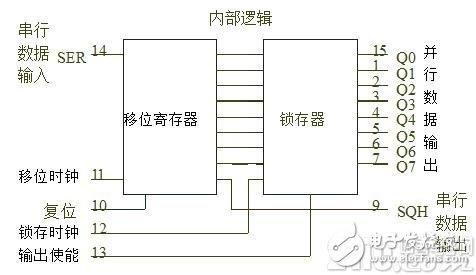
74HC595A internal logic structure
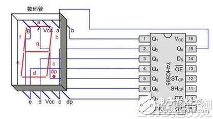
74HC595 and digital tube connection
The serial shift register receives the external input serial data, and can perform serial data output on the one hand, and provides 8-bit parallel input data to the latch at the same time, and has an asynchronous reset function; the 8-bit latch can output parallel data in three states. . The chip has two independent clock signals for serial input and parallel output.

74HC595A logic function table
Note: U: unchanged; N: data refresh; Z: high resistance.
2. Application circuit design
The figure below shows the 12-bit LED display application circuit. If the ordinary LED parallel display mode is used, the single-chip interface needs to be extended, and the circuit is complicated and costly. The system uses three 74HC595A chips to achieve 12-bit serial LED display control. In use, under the control of the serial clock, the display bit control code and the segment control code can be serially input into the three chips bit by bit, and then the parallel output is realized by using the latch signal to complete the 12-digit digital display update. The use of this display mode only occupies the three port lines of the single-chip microcomputer, which greatly saves the resources of the single-chip line. With serial data input, the display speed is relatively slow, and the display effect is stable and reliable in actual use, which fully meets the design requirements.
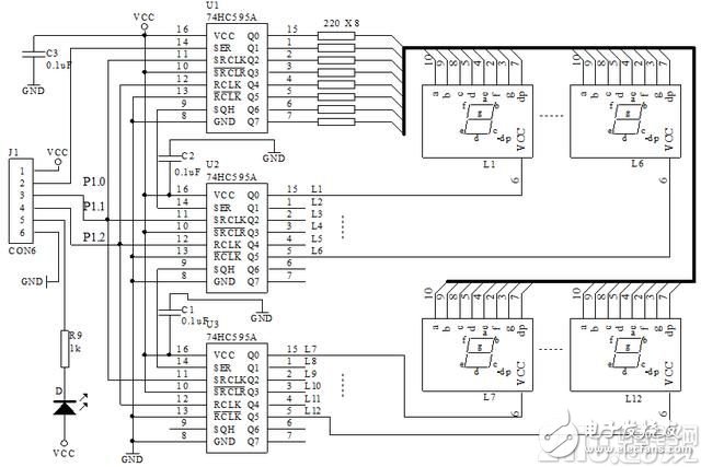
12-bit LED serial display application circuit
The initial bit control code is set to display the first digit tube (common cathode), see the first row of the bit control code in the table below. Each time one bit is displayed, the bit control code needs to be changed to display the next bit. The table below reflects the change of the bit control code. The 1-zone registers R6 and R7 are used to store the processing bit control code.
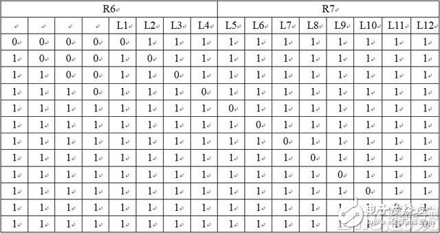
12-bit LED display bit control code formation diagram
3. Show how the program works
This program controls the display operation in a timed manner. The 12-bit display uses dynamic scanning display, and each display display time is approximately 1.67ms, controlled by timer T0. T0 times the time to generate a display interrupt, enters the display interrupt program to display the next bit of data. This display mode can improve the working efficiency of the CPU and accurately control the refresh rate of the display.
4. Interrupt display subroutine application
Prepare a program to display 0, 1, 2, 3, 4, 5, 6, 7, 8, 9, 0, 1 in sequence on a 12-digit digital tube
ORG 0000H
DSDATE BIT P1.0; serial data input
DSCLK BIT P1.1 ; serial shift clock
DSLUCK BIT P1.2; parallel latch clock
DISBUF EQU 51H ; display buffer first address
DS20 EQU 34H ; 20ms timing register (12-bit display counter)
LJMP MAIN; transfer to the main program
ORG 000BH
LJMP TIMINT ; timed display interrupt subroutine
MAIN: MOV SP, #70H ;
MOV 51H, #00H ; preset display buffer
MOV 52H, #01H
MOV 53H, #02H
MOV 54H, #03H
MOV 55H, #04H
MOV 56H, #05H
MOV 57H, #06H
MOV 58H, #07H
MOV 59H, #08H
MOV 5AH, #09H
MOV 5BH, #00H
MOV 5CH, #01H
MOV 08H, #DISBUF ; Zone 1 R0 points to the first address of the display buffer
MOV 0EH, #07H ; set initial control code (1 zone R6)
MOV 0FH, #0FFH ; set initial control code (1 zone R7)
MOV TMOD, #01H; set T0 to 1.67ms timer
MOV TL0, #00H
MOV TH0, #0FAH
MOV DS20, #12 ; display digit counter
SETB TR0 ; start T0
SETB EA; open interrupt
SETB ET0; open T0 interrupt
HERE: SJMP HERE
TIMINT: PUSH PSW; timed display interrupt subroutine, status word is pushed onto the stack
MOV PSW, #08H ; Reset status word, select 1 area working register
PUSH ACC; accumulator is pushed onto the stack
PUSH B ; B register is pushed onto the stack
CLR TR0 ; stop T0 timing
MOV TH0, #0FAH ; Reset the initial value of 1.67ms
MOV TL0, #00H
SETB TR0 ; start T0 timing
MOV R5, 0FH; bit control code to send R4, R5
MOV R4, 0EH
LCALL DIS1; call to display a digital tube program
SETB C ; forming the next bit control code and placing it in zone 1 R6, R7
MOV A, R6
SETB ACC.4
RRC A
MOV R6, A
MOV A, R7
RRC A
MOV R7, A
DJNZ DS20, LOOP1; 12-bit display is finished, no exit, if reset is displayed
MOV DS20, #12; reset display counter
MOV R0, #DISBUF ; reset display buffer pointer
MOV R7, #0FFH ; Reset initial bit control code
MOV R6, #07H
LOOP1: POP B; recovery site
POP ACC
POP PSW
RETI; interrupt return
DIS1: MOV DPTR, #TAB ; Display a digital pipe program, pointing to the segment code table
MOV A, @R0 ; character data to be displayed
INC R0 ; modify buffer pointer
MOVC A, @A+DPTR ; look up the table to display the character segment code
MOV R3, A ; combine segment code and bit control code into 20-bit valid serial code
MOV R1, #0CH ; 20-bit valid serial code is placed in R3, R4, R5
MOV A, @R1
SWAP A
MOV @R1,A
MOV A, R3
XCHD A, @R1
MOV A, @R1
SWAP A
MOV @R1,A
MOV A, R3
SWAP A
MOV R3, A
MOV R1, #20; set serial output counter
DIS0: MOV A, R3 ; R3, R4, R5 are serially shifted and output by R5 high.
RRC A
MOV R3, A
MOV A, R4
RRC A
MOV R4, A
MOV A, R5
RRC A
MOV R5, A
MOV DSDATE, C ; the highest bit is sent to the 595 chip serial input
SETB DSCLK; generates 595 chip serial input signal
NOP
CLR DSCLK ; serial input latch
DJNZ R1, DIS0; 20-digit binary code output is finished, no more continues
SETB DSLUCK; generate 595 chip parallel output signal, characters start to display
NOP
CLR DSLUCK; output character data is latched by 595 chip
RET
TAB: DB 3FH, 06H, 5BH; display segment code table
DB 4FH, 66H, 6DH
DB 7DH, 07H, 7FH
DB 6FH, 00H, 40H
Laptop power adapter charger for Asus:
Laptop Model
Power Adapter
K42F K42JB K42JK K42JR K42JV K52f A52f A42 X52f A52 A52f A52J
19v 3.42a, 5525
K60IJ K50IJ K50I K60I
19v 4.74a, 5525
Our service:
Stable output and high charging efficiency.
Elegant outlook design as original one, touch smoothly and comfortable.
Original charger is good, but as a replacement, our product has more reasonable price when your original charger is broken.
And, the market of the replacement adapters becomes bigger and bigger. People would rather buy a copy one then the original because of the price.
But at the same time, people worry about that they will buy something defective. So the problem comes, how to buy a good quality one with a good price?
As a professional power adapter manufacturer, we have excellent R&D team, skilled staffs and responsible after-sale service. All your benefits can be under protected after you buy products for our company.
Our certificates :ISO9001:2008 & ISO14001:2004 , CCC , CE , FCC , ROHS.
All our products has 1 year warranty. In other words, if you get the dad products which are not damaged physically from us in one year, we will replace you the new one or the whole bulk order.
Asus Adapter,Adapter For Asus,Laptop Adapter For Asus ,Power Supply For Asus
Shenzhen Waweis Technology Co., Ltd. , https://www.waweisasdapter.com