At present, most image surveillance systems use PCs and video capture cards as the main part of the system. Image surveillance system equipment based on embedded technology is still in its infancy in my country, and there is no mature product application. The fundamental reason for this status quo is that when my country is developing such products, there is no unified development standard and shared development platform, and there is no reliable function and performance test standard. The development and technical strength of each enterprise is scattered, which greatly affects the The efficiency and reliability of product development. Compared with similar foreign products, the manufactured products have very different functions and are not competitive. The market is basically occupied by foreign companies. Therefore, it is imperative to develop an embedded system of this type.
System overall schemeIn order to achieve automatic image alarm and image acquisition, this paper designs a moving body detection algorithm. This is because in most cases we are only interested in moving objects in the monitoring area, so that images that only contain static background can be filtered out, thereby reducing This reduces the consumption of limited embedded hardware resources. Since most of the moving objects are people, and this is also the goal of image monitoring, a human body signal detector is added to assist the detection of moving objects to achieve the purpose of reducing the false alarm rate of image alarms. This system mainly integrates devices or chips such as image acquisition, control and storage, forming a real-time image monitoring system with FPGA as the control core. The overall scheme of the system is shown in Figure 1.
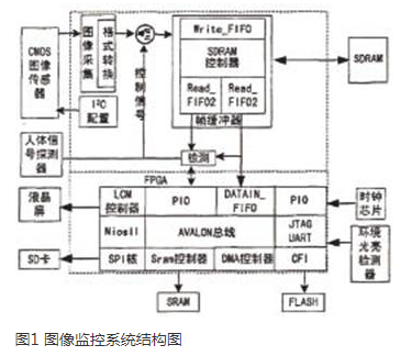
The system workflow is: After the system is powered on, the FPGA automatically loads the program from the external EEPROM, and the I2C module initializes the working parameters of the CIS. CIS inputs image data signals to FPGA, FPGA converts the collected raw data (RAW) into RGB format, frame buffer module (Frame Buffer) writes two adjacent frames of image data into SDRAM each time, and then compares the difference between the two frames If the difference is greater than the set threshold, and the human body detector outputs a high level, it is considered that the movement of the external scene has been detected, and the system will automatically output the captured image to the SD card for storage. Figure 2 shows the workflow of the system.
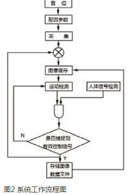
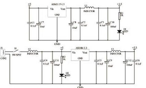
Figure 3 Schematic diagram of power supply circuit
System hardware design and implementationThe amount of data processed by the image monitoring system is relatively large, and the real-time requirements must be met at the same time. Therefore, the on-board circuit needs to select devices with larger capacity and faster speed. The resolution size of one frame of image collected by this system is 640&TImes;480, and the color depth is 24 bits. Two frames need to be cached in SDRAM during detection. Therefore, the capacity of SDRAM must be greater than 1.8M bytes (640&TImes;480&TImes;3&TImes;2=1843200 Byte). Since each pixel has a bit width of 24 bits and NIOS is a 32-bit processor, the bit width of SDRAM is preferably 32 bits. The frequency of the crystal oscillator externally provided to the FPGA must be greater than the 25MHz pixel clock of the CIS. Considering that the detection algorithm requires more logic resources, the on-chip LE of the FPGA must be very rich. In addition, the pins of the FPGA must meet the requirements of external device connection. In this system, the I/O ports of all devices must be connected. FPGA I/O pins must be greater than 150. Since there are many circuit schematics, only a part of them is given here.
Main control chip circuitThe specific model of Cyclone series FPGA device selected by this system is EPlCl2Q240C8. The logic resources are up to 12,060 logic elements (LE, Logic Elements), and the on-chip RAM capacity is 239616 bits. It can fully meet the design requirements of image acquisition. Its core power supply adopts 1.5V, 0.13um craft, low power consumption. Cyclone devices support various single-ended I/O interface standards, such as 3.3V, 2.5V, 1.8V, LVTTL, LVCMOS, SSTL. Cyclone devices have two programmable phase-locked loops (PLL) and eight global clock lines, providing sound clock management and frequency synthesis functions to achieve maximum system performance. Cyclone devices have advanced external memory interfaces, allowing designers to integrate external single data rate (SDR) SDRAM, double data rate (DDR), SDRAM, and DDR FCRAM devices into complex system designs without degrading data access performance. Cyclone series FPGA devices are based on a new low-cost architecture. Cost savings are fully considered from the beginning of the design, so it can provide brand-new programmable solutions for price-sensitive applications.
Power circuitGenerally speaking, due to the needs of chip design and multi-level interface, FPGA devices are divided into two groups of power supplies: VCCINT and VCCIO, that is, core power and I/O power. As the internal wiring of the chip gradually decreases, The core power supply voltage and interface voltage are also getting lower and lower. VCCINT of EPlCl2 device in this design is 1.5V, and VCCIO is 3.3V. There are currently three power solutions in general: linear regulator power (LDO), switching regulator power and power modules.
The LDO linear regulator is suitable for step-down conversion, and the specific effect is related to the input/output voltage ratio. From the basic principle, the LDO adjusts its internal resistance according to the change of the load resistance, so as to ensure that the voltage at the regulated output terminal remains unchanged. Its conversion efficiency can be simply regarded as the ratio of output to input voltage.
Due to the linear regulation principle, the LDO essentially has no output ripple. Compared with LDO, DC/DC regulator output ripple voltage is larger, the instantaneous recovery time is slower, and electromagnetic interference (EMI) is easily generated. The system power input voltage is 5V, and the 3.3V voltage power supply part adopts AS1084; in addition, the 1.5V power part required for the PLL operation of the FPGA is realized by AMS1117-1.5 LDO.
Since Altera's PLL is implemented by an analog circuit, it is more sensitive to power supply noise, so when designing the PCB, some special treatments should be done on the power supply to the PU. Even if the PLL is not used in the design, it must be powered.
The input and output interface voltage of the EPlCl2F400C8 chip selected in this system is 3.3V, and the core voltage is reduced to 1.5V, which can reduce power consumption and is beneficial to the stability of the system, but it also brings trouble to the power supply and the selection of other chips. The interface voltage of other chips in the system must be 3.3V, at least compatible with 3.3V. The main issue that needs to be considered in power supply design is whether the power is satisfied.
SD card interface circuitAmong various storage devices, SD cards are not only compact, but also have low power consumption. In addition, the capacity of common SD cards on the market can reach more than 2GB, so they are very suitable for embedded image storage with strict requirements on volume and power consumption. As shown in Figure 4, the two data lines DAT0 and CMD of the SPI are connected to pull-up resistors respectively. This is to make this circuit compatible with the interface of the MMC card. The power supply of the card is controlled. This is to prevent the SD/MMC card from entering an indeterminate state. The card can be reset by re-powering on the card without pulling out the card. The controllable circuit uses a P-type MOS tube, which is controlled by the GPIO port SDPC of the FPGA. When the SDPC outputs high level, the MOS tube is turned off and does not supply power to the card; when the SDPC outputs low level, the MOS tube is turned on, and VCC3V3 power supply to the card powered by. Consider that when the tube is turned on, the voltage drop between the drain and the source should be small enough (to ensure that the working voltage of the SD/MMC card is within the allowable range), and the allowable current of the tube should also meet the requirements of the card. Generally, a SD/ The maximum current when the MMC card is working is usually about 45mA, so the selected MOS tube requires a current of about 100mA. The purpose of using 2SJ355 is that when it is turned on, the pressure drop on the tube is relatively small.
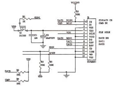
Figure 4 SD card circuit schematic
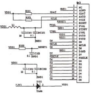
Figure 5 Schematic diagram of image sensor circuit
The card detection circuit includes two parts: whether the card is completely inserted into the card socket and whether the card is write-protected. The detection signal is output in a level mode from the two pins of the deck. When the card is inserted into the card socket and inserted in place, SDIN (pin 10) will output low level due to the internal contact of the card socket connected to GND; when the card is pulled out, this pin will output due to the presence of the pull-up resistor R2 High level, the output is detected by the input pin of FPGA. The detection principle of whether the card is write-protected is the same as the detection principle of whether the card is completely inserted into the card socket.
Image sensor circuitThe image acquisition module at the input end is a CMOS image sensor. Compared with CCD sensors, CMOS sensors are not only much cheaper than CCD products. Moreover, CMOS sensors can easily achieve a high level of integration (such as CMOS is widely used to shoot micro cameras in mobile phones), and CMOS sensors have the advantage of ultra-low power consumption. The image acquisition of this system is used in the monitoring field. The quality of the image is not very high, and the power consumption of the sensor must be very low, and it can directly output the data format required by the system, so the image acquisition part of this system uses CMOS image sensor.
In this design, Micron Technology’s MT9M011 CMOS image sensor is used. MT9M011 is an SXGA (super extended graphics array) standard 1/3-inch active digital image sensor with an effective image sequence range of 1280× 1024, combined with the functions of many digital cameras such as window viewing, row and column jumping, snapshot mode, etc., programmable operation can be realized through a two-wire serial port, and it has the characteristics of low power consumption. The on-chip A/D converter will provide the output precision of each pixel I/O bit, the frame valid and line valid signals will be output on specific pins, and the valid data of the pixel clock synchronization response will also be provided.
NiOS system software design and implementationThe software design of this system is written in C language using the hardware configuration module (HAL) function support provided by Altera's software integrated development tool IDE. After the system is started, the initialization work is carried out. The initialization procedure mainly completes the initialization of the DMA channel and the clearing of the FIFO buffer of the FIFO control interface. Then the system enters the main loop state and detects the keystrokes. When DETECT is detected, the FIFO control interface starts to save data, and when data_avaible is detected to be valid, a DMA transfer is started. In this way, until SAVE_DONE is detected, the image data collection function is realized.
UART transmission program designThe uart transmission program is mainly to transmit image data to the computer for display and debugging. On the PC side, the image is displayed through the serial port receiving tool and Matlab. In the Nios II system, UART transmission (uart 0) can be performed through the standard library functions of ANSI C file operation, that is, UART is handled as a file. The execution process is: open the peripheral UART and obtain the peripheral handle-fopen (); write data outward-fWrite (); close the peripheral-fclose ().
Program Design of SD Memory CardSD card programming includes two parts: driver and file system. The two parts are connected through the interface function of the file system. The driver includes a hardware configuration module and a command application module. The hardware configuration module includes the hardware environment configuration for accessing the SD card, the basic functions of the SPI interface to realize communication, the initialization of memory variables and the processing of SPI interrupts. The command application module provides read data and write data functions for accessing the SD card.
in conclusionThis article mainly completes the design of embedded image monitoring system, which overcomes the shortcomings of analog image monitoring technology and has strong application prospects in ordinary homes and temporary workplaces. These fields generally have not very high requirements for video transmission indicators, but they are required to be portable, and have low power consumption (such as temporary occasions), small size, low power consumption, low cost, fast speed, good stability, etc. Features, can effectively overcome the shortcomings of traditional computer-based monitoring systems. The system can be used as an intelligent component "embedded" into various application systems. If it is equipped with a network interface and connected to a computer system, a monitoring network system can be formed, which is a relatively independent OEM component.
Budget Laptop
Everyone want a budget laptop. There are different level according to application scenarios. 14 inch Budget Laptop For Students for your elementary project, 10.1 inch Low Budget Laptop for kids play or online learning, 15.6inch celeron j4125 Budget Laptop For Programmers, 14inch budget i5 laptop for your business projects, 15.6inch budget i7 laptop for university students, officers who love bigger screen and performance focused, etc. Of course, other type laptops also optional, like Yoga Laptop , 2 In 1 Laptop, android laptop, etc
As a professional manufacture of custom laptop, Android Tablet, Mini PC , All In One PC, we can provide unique and satisfy oem service. What you need to do is kindly share the exact parameters and special points care more, thus we can provide solutions accordingly.
When you have tender, you can contact us and send the parameters list require, then will provide the most matched one for you. More simple way is that you share your budget, design, delivery time , etc. Believe you can always get a right solution here.
Budget Laptop,Budget Laptop For Students,Low Budget Laptop,Top 10 Budget Laptops,Budget Laptop For Programmers
Henan Shuyi Electronics Co., Ltd. , https://www.shuyicustomlaptop.com