1 Introduction
This paper describes a method for operating the high-capacity NAND FLASH chip VDNF2T16VP193EE4V25 of the company by FPGA. The ALTERA company's FPGA chip is used in the design, and the self-built IP is used to build the hardware platform to realize the NAND FLASH driver. The design can also be ported to other FPGAs and can be used in a variety of embedded electronic systems. NAND FLASH is widely used in electronic systems as data storage. Field programmable gate arrays (FPGAs) have been widely used in various high-end electronic systems. The flexible hardware logic of the FPGA enables read and write operations on NAND FLASH. In this paper, a driving method of NAND FLASH based on NIOS II soft core is described.
2. Introduction to VDNF2T16VP193EE4V25
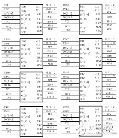
Orbit's VDNF2T16VP193EE4V25 is a 2Tb, 16-bit wide NAND FLASH with an internal 8-substrate topology. The topology is as follows:

Figure 1 VD1D8G08VS66EE8T7B topology
Its main features are as follows:
Ø total capacity 2Tb;
Ø Bit width: 16 bits;
Ø SLC;
Ø Compatible with ONFI2.2;
Ø Package: PGA193;
Ø Power supply: +3.3V (VCC), +1.8V (VCCQ).
3. Controller design of VDNF2T16VP193EE4V25
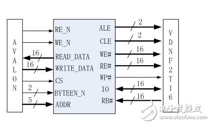
The high-capacity NAND FLASH controller design includes an IP core design. It is based on the NIOS II AVALON bus. The AVALON bus is compatible with most memory interfaces, and the IP core transfers AVALON bus timing to NAND FLASH for read and write operations on NAND FLASH.
IP logic mainly has chip select signal generation, transfer of control signals such as ALE, CLE, RE, and WE. The RE and WE signals can be RE and WE signals of the AVALON bus; CLE and ALE are controlled by the lower 2 bits of the bus address; the number of chip selects can be decoded according to the BYen signal of the AVALON bus.

Figure 2 Controller Functional Block Diagram
/ / write signal
Assign nand_wr_n = {avalon_wr_n, avalon_wr_n, avalon_wr_n, avalon_wr_n};
//Read signal
Assign nand_rd_n = {avalon_rd_n, avalon_rd_n, avalon_rd_n, avalon_rd_n};
//ALE signal, using address 0
Assign nand_ale = {avalon_add[0], avalon_add[0]};
//CLE signal, using address 1
Assign nand_cle = {avalon_add[1], avalon_add[1]};
//chip select signal
Assign nand_cs_n[0] = temcs[0]|avalon_byteen_n[0];
Assign nand_cs_n[1] = temcs[0]|avalon_byteen_n[1];
......
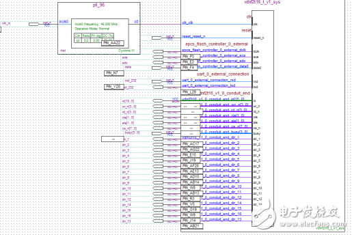
After the IP core design is completed, the hardware platform is built by QSYS. The soft core of the QSYS system has EPCS, UART and NAND FLASH interfaces. The Quartus II software is used to compile the principle block to generate hardware information.

Software programming of QSYS with Nios II Software Build Tools for Eclipse enables NAND FLASH drivers.
//NAND FLASH data register address definition
#define NandFlashDataReg0 (VDNF2T16_V1_0_BASE)
//NAND FLASH ALE register address definition
#define NandFlashAddReg0 (VDNF2T16_V1_0_BASE+4)
//NAND FLASH CLE register address definition
#define NandFlashCmdReg0 (VDNF2T16_V1_0_BASE+8)
......
The following is the information for reading the ID and bad blocks:
************************************************** ****************
The cs=0 NAND_FLASH's ID is Right , The ID is=0x2c881a7a9000
************************************************** *********************
This cs=0 FLASH's Bank=0 have 5 BadBlocks:
The num=0 Bank LUN1's num=90 is BadBlock.
The num=0 Bank LUN1's num=91 is BadBlock.
The num=0 Bank LUN1's num=1738 is BadBlock.
The num=0 Bank LUN2's num=90 is BadBlock.
The num=0 Bank LUN2's num=91 is BadBlock.
The Number of Bank's Valid Block is Right.
......
Thermal Relay is used to protect AC three-phase asynchronous motor/electric motor against overload and open phase. Korlen electrical appliances produce thermal relay switch in wholesale,being a good thermal overload relay suppliers from china. We also offers Manual Motor Startor , AC Contactor, led light, Circuit Breaker etc.
Thermal Relay,Latching Relay,Reed Relay,Polarized Relay
Wenzhou Korlen Electric Appliances Co., Ltd. , https://www.korlen-electric.com