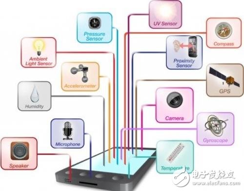
From screen rotation, motion detection, digital compass and 3D games, to augmented reality (AR), digital image stabilization, location service (LBS), indoor and multi-floor blind zone navigation, accelerometers, gyroscopes, barometers The sensors represented represent an important role in the era of smart connectivity. So, an obvious challenge for smartphone designers is how to manage the rapidly growing sensors in their phones?
limited resources
It is not new to manage sensors using the mobile application processor or the "Sensor Hub" with MCU/ASSP/ASIC as the core. But Subra Chandramouli, marketing manager for consumer mobile electronics at Lattice, believes that with each sensor added, limited system GPIO resources can become the first stumbling block that hinders designers from moving forward; second, different sensors bring The requirements of specific interfaces, which limit the number of sensors that an AP or MCU can support, increase the complexity of the design and extend the product development process. Third, because the absolute number of sensors is increasing, they are constantly collecting time sensitive. In the process of type data, AP is one of the biggest consumers of system power consumption.

In order to address these limitations and address increasing power, cost and size targets, in the design of multi-sensor mobile electronics, some smartphone developers have begun to abandon the traditional approach of connecting sensors to APs/MCUs. Choose to use low-density field-programmable gate array (FPGA) products optimized for mobile applications to separate sensor management functions from application processors that consume large amounts of power. An example is the ultra-low-density iCE40LM FPGA that Lattice has announced today.
Flexible solution
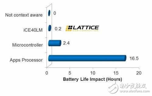
The iCE40LMFPGA features a strobe signal generator with hard IP, I2C and SPI interfaces. The 25-ball/16-ball WLCSP (wafer-level chip) package technology allows the iCE40LM family to be packaged in a minimum package size of 1.4mm x 1.48mm x 0.45mm. It integrates many advanced features on a single chip such as IrDA, bar code emulation, breathing LEDs, and logic that can be used to add user-defined functions. More importantly, the power consumption of the iCE40LM series is less than 1mW. The power consumption of the iCE40LM FPGA solution is about 100 times lower than that of the traditional single AP solution, and the design power consumption of the AP+MCU is 10 times lower.

iCE40LM sensor management solution reduces power consumption by several orders of magnitude
Subra Chandramouli said that by using low-density FPGA products as sensor connectivity hubs, designers can effectively separate computationally intensive sensor management functions from the computing core of mobile devices, not only faster than coprocessors and ASSPs, but also greatly reduced Power consumption and board area. Huge design flexibility is said to be another big advantage for such products.
In addition, because each I/O of the FPGA is configurable, designers can easily change the design to support new interface requirements through any form of interface input from the FPGA. Lattice believes that this new free way allows designers to quickly and easily exchange sensors with different performances, regardless of their interface requirements, without worrying about changing code in the processor subsystem or redoing boards. The interface between the application processor and the FPGA hub that was locked early in the product design can still be significantly modified during the design process without affecting the product development plan.
Equally important, this new approach brings considerable benefits to power consumption. In the past two decades, typical FPGA static power consumption has dropped dramatically, from 0.5W to less than 50μW today. Thus, as an event-driven system, an FPGA-based hub can instantly respond to incoming sensor data and effectively reduce the load on the application processor's time-consuming sensor management and control operations.
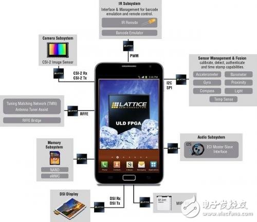
As an example, the block diagram below illustrates an application that uses ICE40 FPGAs in recent cell phone designs. By separating the timing-critical "detection, decision, and verification" functionality from the application processor, the application implements I/O expansion and multi-sensor management applications that help reduce application processor uptime and power consumption.

Lattice iCE40LM for I/O expansion and multi-sensor management applications in handset design
In addition to providing sensor reference designs based on the iCE40LM FPGA, Lattice also works with major sensor technology IP vendors to provide key IP including bar code emulation, infrared remote control and sensor management. At the same time, Lattice iCEcube2 design software and Lattice Diamond Programmer v3.0 support all iCE40 devices, providing mobile device designers with an efficient, integrated development environment.

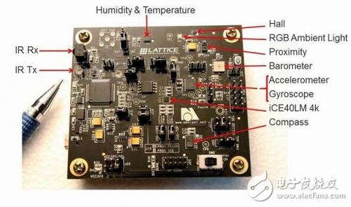
iCE40LM sensor daughter card
5.1 Home Theater Speaker,Home Theatre 5.1,Wireless Surround Sound Speakers,Bluetooth Surround Sound System
GUANGZHOU SOWANGNY ELECTRONIC CO.,LTD , https://www.jerry-power.com