Summary
In the development process of C6000 DSP, optimization is an indispensable part, which can be divided into system, algorithm, code and memory optimization according to different objects. Usually, developers are familiar with their own code, which will be modified from the first three aspects to improve the overall performance, but for the optimization of memory, especially cache, because it involves the architecture of the chip itself, the maintenance of Cache is done automatically by DSP. Users can't usually intervene, so it seems that there is no way to start; considering these practical problems, TI's 7.0 series compilers support the use of Cache Layout Tools to optimize C6000 code. Through this series of tools, you can It is very easy to improve the performance of L1P Cache. This article describes in detail how to use the tool.
1 Introduction
At present, there are more and more users using TI DSP. In the C6000 series DSP, C64x, C64x+, C66x, etc. are included. In the development process of C6000 DSP, in order to make full use of the computing resources of DSP, it is necessary to optimize the user program, which can be divided into system, algorithm, code and memory optimization according to different objects. Usually, developers are familiar with their own systems and code, which can be easily modified from the first three aspects to achieve overall performance improvement, but for memory, especially cache optimization, because it involves the architecture of the chip itself, Cache Maintenance is done automatically by the DSP, and the user usually can't intervene, so it seems that there is no way to start; considering these practical problems, from the 7.0 series of compilers from TI, support for optimizing the C6000 code using the Cache Layout Tools. A series of tools that can easily improve the performance of L1P Cache. This article details how to use the tool.
2.C6000 DSP kernel caching mechanism
The memory structure of the C6000 system is shown in the figure below.

Figure 1. C6000 memory structure
The memory is divided into three levels: the first level is L1, including data memory (L1D) and code memory (L1P); the second level is code and data shared memory (L2 and MSMC SRAM); the third level is external memory, mainly DDR Memory. The Cache functions of L1P, L1D, and L2 are performed by the corresponding L1P controller, L1D controller, and L2 controller, respectively.
In the C6000 DSP, we usually configure L1P as Cache. When the CPU issues the command, it will first search from L1P. If L1P is not found, it will be searched in the next level of Cache or Memory. When the required address is found. , then read it into L1P, the CPU reads the execution from it.
Because the size of the L1P Cache is limited (32KB for example), and the user memory space is generally larger than 32KB, a mapping method must be adopted to enable all addresses to be cached by L1P. In the C6000 DSP, the L1P Cache uses the address directly. Mapping, the address accessible by all DSP cores can be obtained by modulo the L1P Cache size (32K) to get the offset value of the address in the L1P Cache.
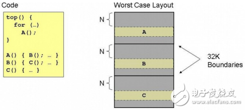
If the user code is not properly arranged in memory, repeated content replacement may occur in the L1P Cache. The example in the figure below is an extreme case.

Figure 2. Incorrect arrangement of functions
In the TOP function, the FOR loop repeatedly calls the A function, and the three functions A, B, and C are in the same memory address distribution, and the offset address of the 32KB boundary is the same. Therefore, A, B, and C will correspond to the same one in L1P. CACHE location; its operation process is as follows
When executing A, the CPU needs to call the A function to the position of the Cache offset value N;
A calls B, then transfers B to the location of the Cache offset value N, overwriting the code of A;
B calls C, at this time, it is called C to the location of the Cache offset value N, covering the code of B;
C returns, the next loop calls A to the code in the Cache that overwrites C.
DSP check L1P, L2, DDR access speed is very different, access to L1P is usually completed in 1 clock cycle, while L2 requires 3-5 cycles on average, DDR access takes more time, so we should try to avoid In the above case of repeatedly overwriting the Cache, the replacement of the function in the Cache is reduced as much as possible.
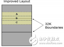
How to solve this problem? The best solution is to continuously discharge A, B, and C in memory, so that the number of operations on the Cache will be minimized, and the execution efficiency can be effectively improved, as shown in the following figure, as long as A, B, and C are total. The size does not exceed 32KB, their offset value in the Cache is continuous, and no overwrite occurs. Even if the sum is greater than 32KB, the replacement is only a part exceeding 32K.

Figure 3. Correct arrangement of functions
3. Memory optimization tool
Through the above mechanism, it can be seen that the optimization of L1P Cache mainly analyzes the function call relationship and its distribution in memory. Due to the increasing complexity of user code, it takes a lot of time to manually analyze code call relationships and address arrangements. Therefore, starting with the 7.0 series of compilation tools, TI provides a set of Cache Layout Tools to help users solve this problem quickly and easily.
The principle of the tool is to open the option to generate analysis information when the user compiles the program. The compiler will automatically add the analysis record code to the user program. After that, the user runs the executable file on the TI DSP simulator or DSP chip, and the built-in analysis code. The user's function call relationship and the number of calls are automatically recorded. The more cases you run, the more detailed the information will be, and the better the optimization will be.
After getting the function runtime information, you can use the compiler tool to analyze it, generate the order of the function arrangement, and finally input the arrangement order into the compiler to recompile the original code, and the generated executable file is optimized. Through the memory arrangement, the specific operation can refer to the following examples.
4. Example tutorial This example is mainly composed of three C files.

In the example, the DSP counter TSCL is used to count the number of cycles, and the subfunctions are placed in the sub directory.
The steps to use the example are as follows.
Compile code
This instance is compiled using the TI compiler. To generate information for the profile, you need to add the --gen_profile_info option at compile time. If you use the command form, run the Compile.bat file from the command line. The specific parameters of cl6x can refer to spru186 and spru187. You can find them in the compiler installation directory, such as C:\Program Files(x86)\ Texas Instruments\C6000 Code Generation Tools 7.3.9\doc.
At the same time, OBJ and ASM files are generated in the directory. This has little to do with our experiment and can be ignored. The out file is an executable file that needs to be downloaded to the chip for running, and the map file is used to help us locate the memory address where the profile information is stored.
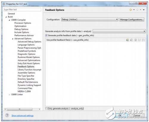
If the user uses the CCS compilation tool, you need to specify the Feedback option in the properties of the Build, and then compile normally to generate the executable file carrying the analysis code.

Figure 4. CCS initial compilation options
RJ45 Jack.China RJ45 Jack Crimping,RJ45 Jack Datasheet,RJ45 Connectors HSN Code,RJ45 Connectors 100 Pack Price, we offered that you can trust. Welcome to do business with us.
Antenk Modular Jacks are a complete line of PCB and wire leaded jacks which are UL and CSA approved and meet all required FCC rules and regulations. Antenk offers a multitude of sizes (4P2C thru 10P10C) with styles including single, ganged and stacked versions with options of ferrite or magnetic filtering and or metal shielding. Jacks with integral LED`s,These jacks are available in thru-hole or SMT mounting.
RJ45 interface can be used to connect RJ-45 connectors. It is suitable for the network constructed by twisted pair. This port is the most common port, which is generally provided by Ethernet hub. The number of hubs we usually talk about is the number of RJ-45 ports.
RJ45 is a type of different connectors (for example: RJ11 is also a type of connector, but it is used on the telephone); there are two different ways to arrange the RJ-45 connector: one is white orange, orange, white green, blue, white blue, green, white brown, brown; the other is white green, green, white orange, blue, white blue, orange, white brown, brown; therefore, there are also wires with RJ45 connector There are two kinds: straight line and interleaved line.
The RJ-45 port of the hub can be directly connected to terminal devices such as computers and network printers, and can also be connected with other hub equipment and routers such as switches and hubs. It should be noted that when connecting to different devices, the jumper method of twisted pair cable used is different.
RJ45 Jack Crimping,RJ45 Jack Datasheet,RJ45 Connectors HSN Code,RJ45 Connectors 100 Pack Price
ShenZhen Antenk Electronics Co,Ltd , https://www.antenkwire.com