introduction
Artificial neural networks have been well applied in many fields, especially network applications with distributed storage, parallel processing, self-learning, self-organization and nonlinear mapping. Embedded portable devices are also increasingly being used, mostly embedded applications based on ARM cores and field programmable gate array FPGAs. An artificial neural network FPGA processor can perform arithmetic processing on data. In order to realize a portable neural network processor integrating data communication, operation control and data processing, it is necessary to design an embedded ARM core and a field programmable gate array. The master-slave structure processing system of the FPGA meets the requirements.
1 artificial neural network processor
1.1 Artificial Neural Network Model
Artificial neural networks are an information processing system based on mimicking brain function. It is actually a complex network system formed by a large number of very simple processing units (or neurons) through a wide range of interconnections. The earliest neuron model is the MP model, which consists of input X, connection weight W and threshold θ, activation function f, and output O, as shown in Figure 1.

Figure 1 MP model of artificial neurons
The output of neuron j is:

Where: netj is the net input of neuron j, xi is the input of neuron j, wij is the weight of neuron i to neuron j, θj is the threshold of neuron j, and f() is the net input of neuron and The transformation function between the outputs is called the activation function. [1]
Later various network models are basically composed of these factors, such as the three-layer BP neural network model of Figure 2.
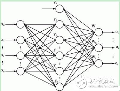
Figure 2 Three-layer BP neural network model
The standard learning algorithm for the three-layer BP network is as follows [2]. When the network output and the expected output are not equal, there is an output error E, which is defined as follows:
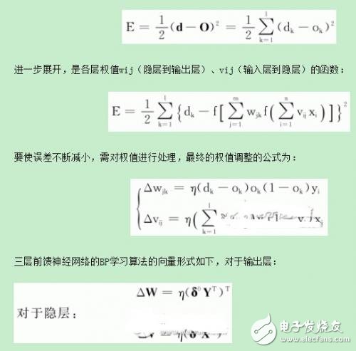
It is easy to see that the weight adjustment formulas of each layer are determined by three factors, namely the learning rate η, the error signal δ output by the layer, and the input and output signal Y (or X) of the layer. Wherein, the output layer error signal is related to the difference between the expected output of the network and the actual output, which directly reflects the output error, and the error signals of the hidden layers are related to the error signals of the previous layers, and are layer-by-layer back-transfer from the output layer. Come over.
The process of training and learning of neural network is to continuously adjust the weight of each node to minimize the output error, and finally obtain stable and reliable weights to realize the predetermined function of the network.
1.2 FPGA implementation of artificial neural network
The algorithm formula actually implies various kinds of operation processes. The multiply-accumulate calculation, the activation function and its derivative calculation and logic operation are three essential operations. Therefore, the implementation of FPGA is mainly the design and connection of various operators. The processor has to deal with various types of data, sample data X (training samples, actual samples), network parameters (learning rate η, number of neurons per layer n, etc.) and weight W are essential. The network parameters and initial weights are used to initialize the network, the training samples are used to train the network learning, and finally the actual samples are processed in the network application phase.

Figure 3 Operational module and data storage structure diagram of neural network
Figure 3 shows the main part of the FPGA neural network processor: the memory module and the arithmetic module. According to the structural characteristics of the network, the connection weight is at the connection of each neuron node, and corresponds to the respective weight operation structure, which is distributed, so the distributed memory WM stores the weight data; the sample data is unified from the network. The input layer enters the network, so the sample data is stored in the DM; the MAE is the arithmetic part of the processor.
2 communication hardware design
2.1 system overall architecture
The overall structure of the system is shown in Figure 4, which is divided into two parts: ARM and FPGA. The ARM side has two functions: one is to read the existing data from the memory, download it to the FPGA through DMA, download the data to different storage devices and storage space according to the data type; second, control the FPGA, mainly Various interrupt operations. The function of the FPGA side is to receive the data transmitted by the ARM, store the data, and perform arithmetic processing under the control of the microprogram controller, and finally upload the result to the ARM.
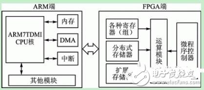
Figure 4 system overall structure block diagram
The ARM side is based on the S3C44B0X chip and externally expands various types of devices. The S3C44B0X is a 16/32-bit microprocessor from Samsung. It integrates the ARM7TDMI core on-chip and integrates a wealth of peripheral function modules to provide a low-cost, high-performance solution for embedded devices.
The S3C44B0X has a 4-channel DMA controller, two ZDMAs connected to the SSB (Samsung System Bus), and two BDMAs connected to the interface layer between the SSB and the SPB (Samsung Peripheral Bus). Where ZDMA can transfer data from memory to memory, memory to I/O devices and I/O devices to memory. The DMA operation is initiated by S/W or a request from an external request pin (nXDREQ0 /1). [3]
In DMA operation, the DMA control is implemented by configuring the DMA Special Function Register, as shown in Figure 5.
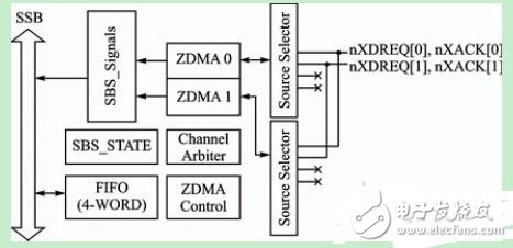
Figure 5 ZDMA controller block diagram
The FPGA side consists of an FPGA chip and an expansion memory. Different storage structures are designed according to different types of processing data, as listed below. The structural parameters of the neural network are stored in the control register group. The initial weights and stable weights are stored in the distributed memory. Other parameters (learning rate, learning rate adjustment factor, etc.) are stored in the special register group A, and the processing results are stored in the special register. In group B, the sample data is stored in the extended memory SD card.
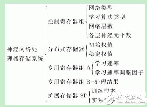
The above described memory banks, except for the extended memory, are all designed inside the FPGA chip. The use of this design is based on the use of FPGA on-chip storage resources: 1 FPGA configuration file occupation; 2 distributed memory occupation; 3 various register groups occupied. When the amount of sample data is large, it takes up a relatively large space, and the FPGA chip cannot be satisfied. Therefore, the sample data cannot be stored on the slice but stored in the extended memory.
2.2 hardware connection
It is easy to find from the above description that the communication object of the ARM chip is a bank on the FPGA chip based on the SRAM process. Therefore, when the FPGA chip is used as a storage device, the ARM chip can be directly connected thereto. The schematic diagram of the connection between ARM and FPGA hardware is shown in Figure 6.
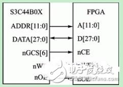
Figure 6 ARM and FPGA hardware connection diagram
The address bus connection between ARM and FPGA's on-chip banks is set to 12 bits, sufficient for storage and addressing needs.
The data bus has a width of 28 bits. The data accuracy of the neural network processor is 16 bits [4], and the FPGA sample data register also has the address data of the 12-bit external extended memory, so the width of the entire data bus is the sum of the two. In addition to the sample data registers, the data lines occupy the lower 16 bits of the 28-bit data bus.
The control bus includes a chip select line nGCS6 and a read/write control line on the ARM side. Configuring the corresponding registers of ARM activates BANK6 (FPGA on-chip bank) and read/write data.
Hardware connections can be divided into two areas depending on where the data is stored. As shown in Figure 7.
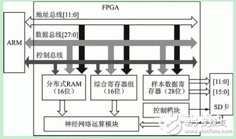
Figure 7 shows the hardware connection of the FPGA end
First, the storage location is an external expansion memory on the FPGA side. 1ARM and FPGA are directly connected through 12-bit address bus, 28-bit data bus and control bus, and data is written into sample data register. 2 sample data register 28-bit data according to 12-bit address data, 16-bit sample data, through the 12-bit address bus between the FPGA and the external expansion memory, 16-bit data bus, under the control of the storage control module, write the sample data Into the expansion memory. Therefore, the sample data register is divided into two parts, the lower 16 bits are the sample data, and the upper 12 bits are the storage addresses of the sample data in the external expansion memory, as shown below.

Second, the storage location is the on-chip bank of the FPGA. ARM and FPGA are directly connected through the 12-bit address bus, the lower 16 bits of the 28-bit data bus, and the control bus. The control register group, the special register group, and the distributed memory are connected to these buses.
The on-chip integrated memory system adopts the unified addressing method. The advantage is that the data can be transferred by the DMA method of the ARM chip, which can increase the transmission rate and release the CPU. The external expansion memory is independently addressed by the FPGA, but The design of the address field is integrated with the address of the integrated storage system on the chip, so it is easy to operate.
3 ZDMA control design
The data communication between the ARM side and the FPGA side is shown in Figure 8, which is divided into three phases:
1 Data communication in the network initialization phase: configure network initialization data. a) Perform phase 2, b) for network training, or stage 3 otherwise.
2 Communication in the network training phase: download training sample data, and the training completes uploading stable weights.
3 Communication in the actual application phase: download the actual sample data and upload the processing result.
Each stage is performed in the ZDMA mode. After each phase is completed, an interrupt will be entered, indicating that this phase is completed and the next step is performed.
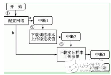
Figure 8 Flow chart of data communication phase
3.1 ZDMA configuration when downloading data
According to whether it is sample data, communication can be divided into two phases: one is non-sample data communication for FPGA on-chip integrated storage system, and the other is sample data communication for FPGA off-chip expansion memory.
This design uses one of the two channels ZDMA0 and ZDMA1. The special function registers associated with ZDMA are:
ZDMA Control Register (1ZDCONn): Mainly used to control the DMA channel, allowing external DMA requests (nXDREQ).
ZDMA0/1 initial source/destination address and count register, ZDMA0/1 current source/destination address and count register.
ZDMAn initial/current source address register (2ZDISRC, 3ZDCSRC): The initial source address is the storage address of the data in the ARM chip memory; the current source address is the memory address of the data to be transferred, and the value is the initial source address + count value.
ZDMAn initial/current destination address register (4ZDIDES, 5ZDCDES): divided into two phases: the initial destination address of the first phase when transmitting non-sample data is the start address of BANK6; the current destination address is changed, the initial destination address + count value. When the second stage transmits sample data, the initial destination address is also the current destination address, which is the address of the sample data register.
ZDMAn initial/current destination count register (6ZDICNT, 7ZDCCNT): The initial value is 0, and the current value is incremented by the number of transmitted data until the number of all data is reached. The transmission of sample data and non-sample data is performed in two stages, each independently.
As can be seen from this process, the problem of the diversity of the storage structure of the FPGA side needs to be considered when configuring ZDMA.
3.2 ZDMA configuration when uploading data
The stability weight and processing result of the neural network processor are stored in the special register group B uniformly addressed on the FPGA. There is no problem of the diversity of the storage structure, so the configuration of the ZDMA is relatively simple when uploading data:
The initial source address is the start address of the special register group B, and the address pointer +1 of the data special register group is transmitted once and is used as the current source address.
The initial destination address is the starting address of the memory block where the data is to be stored, and the data memory block address pointer +1 is transmitted once for each time and is used as the current destination address.
The initial value of the count register is 0, and the value of each time the data is transmitted is +1. When the set target value is reached, the data upload is completed.
Conclusion
This paper first introduces the model and algorithm of artificial neural network and the implementation of FPGA, and designs the data storage system of FPGA on the basis of the analysis of network structure. Then the functions of ARM and FPGA are analyzed. On the basis of this, the two are combined to design a scheme that uses ARM's ZDMA method to communicate with each other.
Our Professional 120W solar panel manufacturer is located in China. including Solar Module. PV Solar Module, Silicon PV Solar Module, 120W solar panel for global market.

120W solar panel, Solar panel, PV solar panel, Silicon solar panel 120W
Jiangxi Huayang New Energy Co.,Ltd , https://www.huayangenergy.com