In the traditional concept, the improvement of the chip process will bring about an increase in performance and a reduction in cost. At the same time, due to the reduction of the chip core voltage, the power consumption is also reduced, which is correct in the 0.13um era.
However, when the process enters the 90nm era, even in the later 40nm or smaller process, there is a slight abnormality, and the power consumption of the chip will be significantly improved.
Since the core voltage of the 40 nm process is further reduced, a negative effect of the voltage drop is that the electric field in the channel in the transistor is weakened, so that the electron moving speed is lowered, and in fact, the propagation delay (tpd) of the transistor is increased. In order to achieve very high performance, chip designers often reduce the threshold voltage (Vth) of the transistor, allowing the transistor to switch quickly for small propagation delays. This Vth is the minimum voltage at which the channel of the transistor begins to conduct.
The reduction of Vth has a serious impact, that is, the leakage current of the transistor increases exponentially with the decrease of Vth, which will greatly increase the static power consumption of the chip. Therefore, the 40nm chip manufacturer needs the performance and performance of the chip. Make a trade-off between the leakage currents that are tolerated.
In general, after the chip enters the 40nm era, the threshold voltage is reduced and the transistor size is reduced, which will lead to an increase in chip leakage current, and this leakage current becomes the main source of static power consumption of the chip, and some even higher. The dynamic power consumption of the chip.
The use of new processes has led to a significant increase in power consumption, which is a common problem facing the semiconductor industry. The problem caused by the increase in power consumption is that the chip will generate more heat in the work. If the heat is not spread out in time, the temperature of the chip will rise. In severe cases, the chip may work abnormally, even Invalid.
FPGA power consumption
A special phenomenon of FPGA devices is that the current at the moment of power-on is relatively large, and sometimes even greater than the normal working current of the chip. This is because the logic and interconnect resources (SRAM process) inside the FPGA are powered on. In an indeterminate state, the result of a current conflict occurs.
If the user does not consider the current at the moment of power-on, the power module cannot provide such a large current. During the power-on process, the power-on curve will not be monotonous, causing the device to fail to power on. So that the chip is not working properly. This power-on current value is usually given in the device manual.
In normal operation, the total power consumed by the FPGA consists of the device's static, dynamic, and IO power. Static power consumption is also called standby power. It is the power consumption when the chip is powered on, but the internal circuit does not work (that is, the internal circuit does not flip). The so-called dynamic power consumption refers to the internal circuit flip. The power consumption consumed; IO power consumption is the power consumed by charging and discharging the external load capacitor when the IO is turned over.
As follows:
Total power consumption = static power + dynamic power + IO power
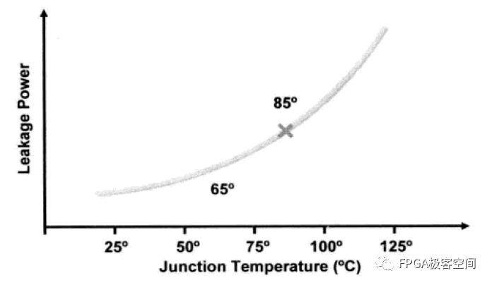
The static power consumption of the chip is the power consumed by the chip in standby mode. It is mainly generated by the leakage current inside the chip. In high-speed 40nm devices (such as stratic IV), the leakage current of the chip is relatively large, so static power consumption becomes the main power consumption, also called leakage power.
A significant feature of static power consumption is that it varies greatly with the junction temperature (TJ) of the device. The larger the TJ, the greater the power consumption; the smaller the TJ, the smaller the power consumption, as shown in the following figure. Therefore, the junction temperature of the control chip can effectively control the static power consumption of the chip.

Relationship between leakage power consumption and device junction temperature
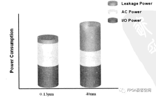
Compared to previous device processes (such as 0.13um), due to the lower core voltage of 40nm devices, the dynamic power consumption of the chip during operation is also reduced.
As for the IO power consumption, since the power supply is separate from the core, the power consumption it consumes does not change much.
The power consumption of different process devices is as follows:

Comparison of power consumption of different process devices
The increase in power consumption is the result of a 40nm high speed chip. If the chip designer reduces the performance specifications of the device, its power consumption will also be significantly reduced. ALTERA 65nm low-cost device CYCLONE III is a good example.
ALTERA provides a method of power calculation in order to enable users to accurately evaluate the actual power consumption of their chips at work.
Power Calculator: Users need to estimate various resource usage in the FPGA, including LE, RAM, PLL, DPS blocks and IO ports, and the clock frequency at which they operate. At the same time, users also need to estimate the flip rate in the working process of various resources, which has a great impact on the dynamic power consumption of the chip. Static power values ​​are also given in the table. In 40nm Stratix IV devices, since the static power consumption is greatly affected by the junction temperature, the calculation table also requires the user to input parameters such as ambient temperature, surface wind speed and heat sink type to estimate the actual standby power consumption of the chip. If the user's design has been completed, the user can output a power estimation file in quartusii and load it into the estimation form to automatically load accurate device resource usage.
Simulation-based power estimation (powergauge): Quartus ii provides a power estimation tool. Before use, the user must first compile the design, then add some stimulus to the design according to the actual situation of the design, and then perform timing simulation on the design in quartusii. Powergauge can estimate the actual power consumption of the chip during the simulation process. This method is usually used to accurately estimate the power consumption of the chip later in the design. It is accurate but time consuming compared to calculating a table.
Fiber Optic Pigtails provide a fast way to make Communication Devices in the field.They are designed,manufactured and tested according to protocol and performance dictated by the industrial standards,which will meet your most stringent and performance specifications.
Bunch pigtails, also known as pigtail bundles, only have a connector at one end, and a broken end of an optical fiber at the other end, which is connected to other optical cable cores by fusion splicing. It often appears in the optical fiber terminal box to connect the optical cable with Terminal Equipment.
Bunch Pigtail is composed of Corning tight-buffered optical fiber that meets full chromatographic specifications, outsourcing aramid fiber reinforced components, and then wrapped with a flame-retardant polyvinyl chloride outer sheath. It is widely used in densely packed transmission lines and terminal equipment. connection.Mainly Used for CATV, LAN/access network, telecommunications network/Gigabit data network testing, medical equipment, other industrial and military applications.
And the most commonly appplied Ribbon Fanout Pigtail includes SC Ribbon Fanout Pigtail and LC Ribbon Fanout Pigtail.
Ribbon Fanout Pigtail, SC Ribbon Fanout Pigtail, LC Ribbon Fanout Pigtail,FTTX
Shenzhen GL-COM Technology CO.,LTD. , https://www.szglcom.com