FPGA is the abbreviation of English FieldProgrammableGateArray, that is, field programmable gate array. It is a product of further development on the basis of PAL, GAL, EPLD and other programmable devices. It emerged as a semi-custom circuit in the field of application-specific integrated circuits (ASIC), which not only solves the shortcomings of custom circuits, but also overcomes the shortcomings of the limited number of gate circuits of the original programmable devices
2. FPGA chip structureFPGA chip is mainly composed of three parts, namely IOE (input output element, input output unit), LAB (logicarrayblock, logic array block, for Xilinx called configurable logic block CLB) and Interconnect (internal connection line).
2.1 IOE
IOE is the physical interface between the chip and the external circuit. It mainly completes the driving and matching requirements of input/output signals under different electrical characteristics, such as from the basic LVTTL/LVCMOS interface to PCI/LVDS/RSDS and even various differential interfaces. 5V compatible to 3.3V/2.5V/1.8V/1.5V level interface, the following is the IOE structure of ALTERA's CycloneIVEP4CE115F29 device
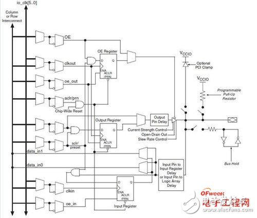
IOE structure diagram of EP4CE115F29 device
FPGA IOEs are classified by groups. Each group can independently support different I/O standards. Through the flexible configuration of software, it can match different electrical standards and IO physical characteristics, and the drive current can be adjusted, and the upper/ Pull-down resistor, CycloneIV device has 8 IOblanks (groups), as shown in the figure below:
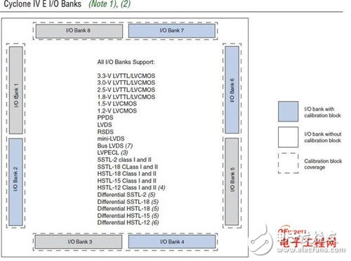
IO group of CycloneIV device
2.2 LAB
LAB is the basic logic unit of FPGA. Its actual quantity and characteristics vary according to the device used. The layout of each LAB of the EP4CE115F29 device includes 16 LEs, LAB control signals, LEcarrychains, Registerchains and Localinterconnect, and its LAB structure The picture is as follows:
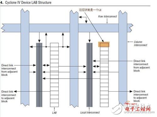
LAB structure diagram
LE is the smallest logic unit of CycloneIV equipment. Each LE is mainly composed of LUTs and registers.
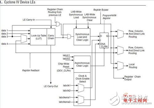
LE structure diagram
The look-up table LUT (Look-Up-Table) is essentially a static memory SRAM. At present, FPGAs mostly use 4-input LUTs, and each LUT can be regarded as a 16x1 RAM with a 4-bit address line. When we describe a logic circuit through a schematic diagram or HDL language, the FPGA development software will automatically calculate all possible results of the logic circuit and write the results into RAM in advance. In this way, when the FPGA is working, each input of a signal for logic operation is equivalent to inputting an address to look up the table, find out the content corresponding to the address, and then output.
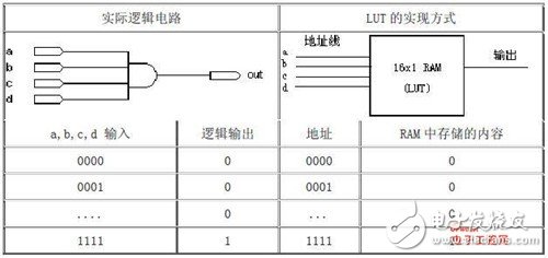
Schematic diagram of the implementation of LUT
2.3 Interconnect
The FPGA internal connection lines are very rich. According to the description of the data manual, there are mainly Rowinterconnect, columninterconnect, Directlinkinterconnect, and Localinterconnect and Registerchaininterconnect (connecting lines between registers) in Figure 3.
The internal connection line connects all the units inside the FPGA, and the length and process of the connection determine the driving capability and transmission speed of the signal reconnection line. In the actual development, the designer does not need to directly select the connection line, the place and router can automatically select the connection line to connect each logic unit according to the topology and constraint conditions of the input logic netlist (which is generated by synthesis), so from the essence In the above, there is a close, direct and direct relationship between the method of using wiring resources and the result of the design.
3. How FPGA worksFPGA uses a small look-up table (16×1RAM) to implement combinational logic. Each look-up table is connected to the input of a D flip-flop (see Figure 4), and then the flip-flop drives other logic circuits or I/O, thus forming A basic logic unit module that can realize both combinational logic function and sequential logic function is implemented. These modules are connected to each other or I/O modules by metal wires. FPGA logic is realized by loading programming data into the internal static storage unit. The value stored in the memory unit determines the logic function of the logic unit and the connection between modules or between modules and I/O, and finally determines The function that FPGA can realize, FPGA allows unlimited programming.
4. FPGA development processSchematic and HDL (HardwaredescripTIonlanguage, hardware description language) are the two most commonly used digital hardware circuit description methods, among which HDL design method has better portability, versatility, module division and reusability characteristics, in the current engineering It is widely used in design. The following development process when familiar with FPGA design circuit is based on HDL.

1) System function design
Before system design, the first thing to be done is preparation work such as program demonstration, system design and FPGA chip selection. According to the task requirements, such as the system index and complexity, the system engineer weighs the working speed and the various resources and cost of the chip itself, and chooses a reasonable design scheme and suitable device type. Generally, a top-down design method is adopted to divide the system into a number of basic units, and then divide each basic unit into the next level of basic units, and keep doing this until the EDA component library can be used directly.
2) RTL-level HDL design
The RTL level (RegisterTransferLevel, register transfer level) refers to not paying attention to the details of registers and combinational logic (such as how many logic gates are used, the connection topology of logic gates, etc.), by describing the flow of data between registers and how to process and control The HDL design method of these data flow models. The RTL level is more abstract than the gate level, but also simpler and more efficient. The biggest feature of the RTL level is that it can be directly synthesized into a gate-level netlist with a synthesis tool, and the RTL level design directly determines the function and efficiency of the system.
3) RTL level simulation
It is also called functional (behavior) simulation or pre-synthesis simulation. It verifies the logic function of the circuit designed by the user before compiling. The simulation at this time has no delay information, and only the preliminary function is tested. Before simulation, you must first use a waveform editor and HDL to create waveform files and test vectors (that is, to combine the input signals of interest into a sequence). The simulation results will generate report files and output signal waveforms, from which you can observe the signal of each node. Variety. If errors are found, return to the design to modify the logic design. Commonly used tools include ModelTech's ModelSim, Symnopsys's VCS, Cadence's NC-Verilog and NC-VHDL and other software. Although functional simulation is not a necessary step in the FPGA development process, it is the most critical step in system design.
In order to improve the efficiency of functional simulation, it is necessary to establish a test platform, testbench, whose test stimulus is generally described in behavior-level HDL language, among which RTL-level modules are synthesizable, which is a subset of behavior-level modules.
4) Comprehensive
The so-called synthesis is to transform the description of a higher level of abstraction into a description of a lower level. Comprehensive optimization optimizes the generated logical connections according to the goals and requirements, so that the hierarchical design is flattened for implementation by FPGA placement and routing software. At the current level, synthesis optimization (Synthesis) refers to the compilation of design input into a logical connection netlist composed of basic logic units such as AND gates, OR gates, NOT gates, RAM, flip-flops, etc., rather than the real gate level Circuit. Real and specific gate-level circuits need to use the FPGA manufacturer's layout and routing functions to generate according to the standard gate-level structure netlist generated after synthesis. In order to be converted into a standard gate-level structure netlist, the HDL program must be written in accordance with the style required by the specific synthesizer. Since the synthesis of gate-level structure and RTL-level HDL program is a very mature technology, all synthesizers can support this level of synthesis. Commonly used synthesis tools include Synplicity's Synplify/SynplifyPro software and comprehensive development tools launched by various FPGA manufacturers.
5) Gate-level simulation
Also called post-synthesis simulation, post-synthesis simulation checks whether the synthesis result is consistent with the original design. In the simulation, the standard delay file generated by synthesis is back-annotated into the comprehensive simulation model to estimate the influence of door delay. However, this step cannot estimate the line delay, so there is still a certain gap between the actual situation after wiring, and it is not very accurate. The current synthesis tools are relatively mature, and this step can be omitted for general designs. However, if the circuit structure is found to be inconsistent with the design intent after placement and routing, you need to go back to post-synthesis simulation to confirm the problem. The software tools introduced in functional simulation generally support post-synthesis simulation.
6) Place and route
Realization is to configure the synthesized logic netlist on a specific FPGA chip, and match the logic and timing of the project with the available resources of the device. Placement and routing is the most important process. Placement reasonably configures the hardware primitives and low-level units in the logic netlist to the inherent hardware structure inside the chip, and often requires a choice between the optimal speed and the optimal area. Wiring is based on the topology of the layout and uses various wiring resources inside the chip to connect various components reasonably and correctly. You can also simply understand the layout and routing as the reasonable configuration of the FPGA internal look-up table and register resources. The layout can be understood to select the optimal combination of resources that can achieve the design netlist. Routing is to maximize these look-up tables and register resources. Connected in an excellent way.
At present, the structure of FPGA is very complicated, especially when there are timing constraints, a timing-driven engine needs to be used for placement and routing. After the wiring is completed, the software tool will automatically generate a report to provide the usage of each part of the resource in the design. Since only FPGA chip manufacturers know the chip structure best, layout and routing must choose tools provided by chip developers.
7) Timing simulation
It refers to the back-annotation of the delay information of placement and routing to the design netlist to detect whether there are timing violations (that is, the timing constraints are not met or the inherent timing rules of the device, such as setup time, hold time, etc.). Timing simulation contains the most complete and most accurate delay information, which can better reflect the actual working conditions of the chip. Since the internal delays of different chips are different, different layout schemes also have different effects on the delay. Therefore, after the placement and routing, it is very necessary to analyze the timing relationship of the system and each module through the timing simulation, estimate the system performance, and check and eliminate the risk of competition.
8) FPGA board level debugging
The configuration file after placement and routing is downloaded to the FPGA through the programmer, and its hardware is programmed. The configuration file is generally in .pof or .sof file format, and the download methods include AS (active), PS (passive), JTAG (boundary scan), etc.
Logic Analyzer (LA) is the main debugging tool for FPGA design, but it requires a large number of test pins, and LA is expensive. At present, mainstream FPGA chip manufacturers have provided embedded online logic analyzers (such as ChipScope in XilinxISE, SignalTapII and SignalProb in AlteraQuartusII) to solve the above-mentioned contradictions. They only need to occupy a small amount of logic resources on the chip and have high Practical value.
| About Bare Wire |
|
Application: Suitable for manufacturing electric motors, windings of electrical equipment, automobile electrical rotors, installation and distribution equipment and other electrical fields.

Name
Conductor
Copper
Dimension(mm)
Rectangular: Thickness(a): 0.90 ~ 5.60
Width(b): 3.15 ~ 16.00
Standard
GB;
Packing
160 kg~180 kg ply-wood spool(250*500; 250*600)
Application
Suitable for manufacturing electric motors, windings of electrical equipment, automobile electrical rotors, installation and distribution equipment and other electrical fields.
Bare wire includes Copper Bar and Aluminium bar
Bare Wire,Bare Copper Wire For Motor,Flexible Bare Copper Wire,Electrical Bare Copper Wire
HENAN HUAYANG ELECTRICAL TECHNOLOGY GROUP CO.,LTD , https://www.huaonwire.com