With the development of information technology, especially the increase in the processing speed of various digital processors, people’s requirements for data acquisition systems are getting higher and higher, especially in some occasions that need to complete a large amount of data acquisition in a very short time. The speed of the acquisition system puts forward very high requirements.
In order to achieve a high-speed, continuous sampling data acquisition system, this article introduces the composition and technical implementation of a data acquisition system based on FPGA + AD7609. Using FPGA as the main module, AD7609 as the data acquisition module, and designed a hardware implementation circuit.
The experimental test results show that the system is flexible in structure, cost-effective, and has strong data collection capabilities. All indicators have met the design requirements and have a wide range of practicability.
2 Realization of data acquisition system2.1 System hardware design
2.1.1 Main control module FPGA
In this design, the FPGA main control module uses Xilinx's Spartan-6 product, the model is XC6SLX9-2FTG256C. The black gold FPGA development board of this series is used in the design, which effectively improves the development and design progress. The structure diagram of the development board system is shown in Figure 1 below.
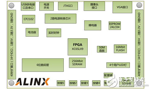
Figure 1 Development board system structure diagram
The FPGA module is the core control part of the entire system. It uses the hardware description language Verilog HDL to program the FPGA to achieve the overall functional requirements of the system.
2.1.2 Data Acquisition Module AD7609
AD7609 is an 18-bit, 8-channel, true differential, simultaneous sampling analog-to-digital data acquisition system (DAS), the device built-in analog input clamp protection, second-order anti-aliasing filter, track-and-hold amplifier, 18-bit charge redistribution Successive approximation analog-to-digital converter (ADC), flexible digital filter, 2.5 V reference voltage source, reference voltage buffer, and high-speed serial and parallel interfaces. Its functional block diagram is shown as in Fig. 2.
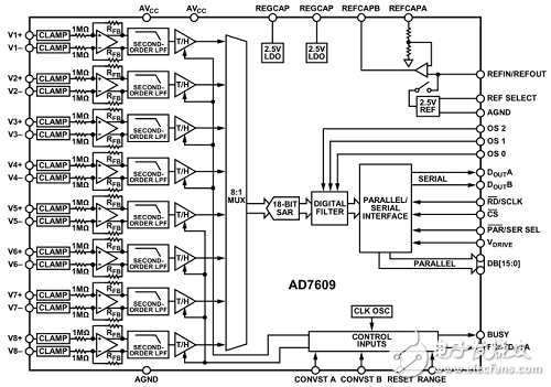
Figure 2 AD7609 functional block diagram
AD7609 is powered by a single 5 V power supply and can handle ±10 V and ±5 V true bipolar differential input signals. At the same time, all channels can be sampled at a throughput rate of up to 200kSPS.
In this design, the working mode of AD is set to serial data acquisition mode, the sampling rate is set to the highest rate of 200kSPS, and the reference voltage is the internal reference mode. The circuit schematic of the design is shown in Figure 3 below.
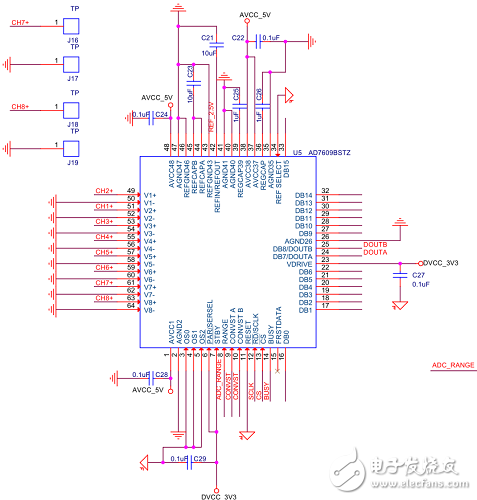
Figure 3 AD7609 schematic design
The control port of AD7609 is connected to the FPGA control module to collect and control data through the Verilog program.
2.1.3 The realization of the hardware circuit
In this design, the AD acquisition circuit was designed using Cadence software, and the actual welding and verification were carried out. The PCB circuit diagram of its printed board is shown in Figure 4 below.
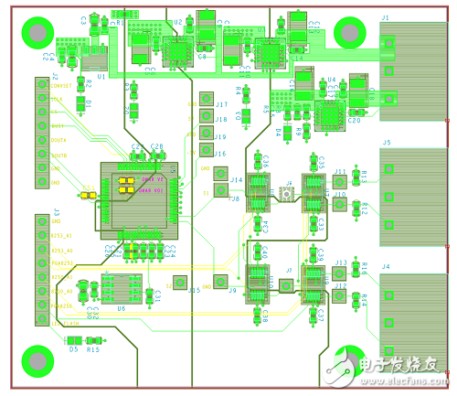
Figure 4 PCB circuit diagram of the printed board
The actual picture of the welding completed and successfully debugged is shown in Figure 5.
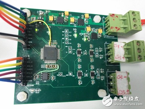
Figure 5 Front-end physical circuit diagram
Among them, the control pin of AD7609 is connected with the IO port of FPGA through a flat cable, and the collected signal is input from the CH1 and 2 ports on the right.
2.2 System programming
2.2.1 Program flow design
In this design, the working mode of AD7609 is configured as serial mode, the sampling rate is 200kSPS, and the corresponding serial mode sampling timing is shown in Figure 6.

Figure 6 Sampling timing diagram of serial mode
Design the AD acquisition conversion program through FPGA, according to AD7609 sampling requirements and working characteristics, designed the AD sampling flowchart shown in Figure 7 below.
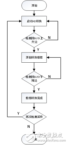
Figure 7 AD7609 sampling flowchart
2.2.2 AD7609 program design
AD7609 can meet the 200kSPS sampling of 8 channels at the same time. In this design, the channels CH1 and CH2 are programmed to control and design. The module interface source program is shown in the figure below.
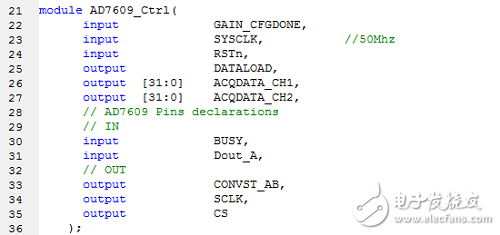
Figure 8 AD7609 module interface program
The source program of AD7609 acquisition control flow is shown in Figure 9 below.
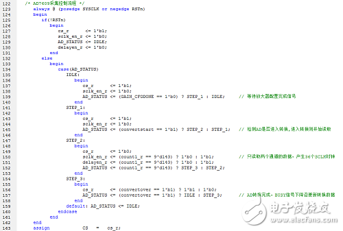
Figure 9 AD7609 acquisition control flow program
The RTL circuit diagram after integrating this module is shown in Figure 10.
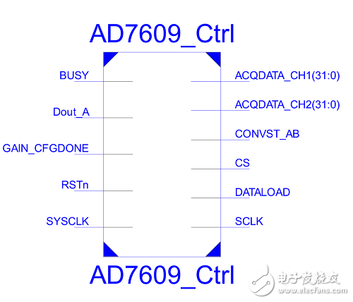
Figure 10 RTL diagram of AD7609 module
2.2.3 Simulation verification
The simulation software inside ISE14.7 is used for simulation verification, and the core test source program is shown in Figure 11.
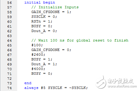
Figure 11 Simulation test source program
The simulation results used are shown in Figure 12 below, which shows that the functional control of the AD7609 is completely realized.

Figure 12 Program simulation verification results
2.2.4 Actual measurement verification
First, configure the ChipScope online debugging software in the work area and add the data to be observed. Then, through the debugging software, download the program to the FPGA of the main control module.
Use ChipScope online debugging software to capture real-time data, verify the correctness of the hardware module, and get the AD7609 data sampling result shown in Figure 13 below.

Figure 13 Sampling results of physical data
In this design, the calculation formula for the numerical conversion of the AD7609 is shown in Figure 14.
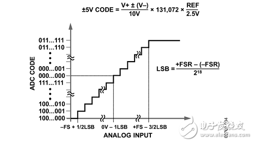
Figure 14 AD7609 numerical conversion formula
The calculation process corresponding to the data in Figure 13 is: (6Af6)H = (27382)D, the sampled value V=27382*10/131072 = 2.08908V, which is consistent with the actual input voltage.
3 ConclusionAfter experimental tests and calculations, the rationality and effectiveness of the system design have been fully verified. Experimental data shows that the data acquisition system is stable and reliable, and realizes continuous sampling of high-speed data.
Dongguan Yijia Optoelectronics Co., Ltd. , https://www.everbestlcdlcms.com