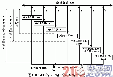
Since its inception in 2000, MSP430 MCU has been favored by many designers with its features of perfect function, ultra-low power consumption and easy development. MSP430 and the traditional 51 single-chip microcomputer are very different in structure. One of them is: In the peripheral interface circuit of MSP430, there is no hardware circuit that controls peripheral read, write, and address latch signals like 51. In line with this interface circuit, MSP430 prefers to use I2C bus and serial interface-based peripheral devices such as ISP. On the other hand, with the development and maturity of I2C technology, its hardware structure is simple, high-speed transmission, and the device is rich, which makes the application of this type of device more and more extensive. Therefore, it is of great significance to study the interface technology of the new single-chip MSP430 and I2C bus. This paper studies this problem, analyzes the principle and method of MSP430 and I2C bus interface, proposes an efficient interface method, and introduces the optimized program. [b]1 MSP430 microcontroller I / O port control features Compared with the 8031 ​​microcontroller, MSP430's I / O port function is much more powerful, and its control method is more complicated. The I/O port of MSP430 can realize bidirectional input and output; complete some special functions such as: drive LCD, A/D conversion, capture comparison, etc.; realize various I/O interrupts. The MSP430 uses a traditional 8-bit port approach to ensure compatibility, ie each I/O port controls eight I/O pins. In order to achieve complex control of each pin of the I/O port, each I/O port in the MSP430 corresponds to a set of 8-bit control registers (see Figure 1). Each bit in the register corresponds to an I/O pin for independent control of that pin. The function and number of registers are determined by the functions and types that the I/O port can perform. [2] Figure 1 is a schematic diagram of the control structure of an I/O port of the MSP430. There are only three control registers for the most basic I/O ports that can only perform input and output functions. Among them, the input register saves the input state; the output register saves the state of the output, and the direction register controls the input and output states of the corresponding pin. P6.6 and P6.7 used to implement the I2C bus interface in this paper belong to this type of port. In addition, some I/O ports can be used not only as basic input and output, but also for other purposes, such as driving control pins for LCDs. The control function registers of such ports implement switching of pin function states. Moreover, there is a type of port that can not only perform the functions of the above two ports, but also implement the interrupt function. This type of port has all the registers in Figure 1, the way the interrupt is triggered and the masking of the interrupt can be controlled by the corresponding registers. The P2.0 used in this article belongs to this type of port and is used to receive interrupts from the LM92.

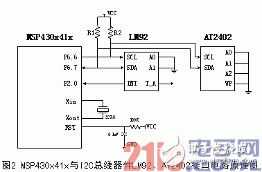
Through the above control structure, the MSP430's I/O port can achieve a very rich function. Not only that, but some of the I/O ports can also be combined with special modules in the MSP430 to perform more complex tasks. If combined with the capture comparison module, serial communication can be realized, and A/D conversion can be realized by combining with the A/D module. In addition, the electrical characteristics of the MSP430 I/O port are also very prominent. Almost all I/O ports have a driving capability of 20 mA. For general LEDs and buzzers, direct drive can be performed without an auxiliary circuit. Many ports have integrated pull-up resistors inside to facilitate interface with peripheral devices. [b]2 MSP430 and I2C bus device interface Through the above introduction, some control features of the I/O port in the MSP430 are known. The following describes how to use these features to implement the interface of the I2C bus. As shown in Figure 2, the P6 of the 41 series MCU is used to generate the timing synchronization signal of the I2C bus; the serial data input and output of the I2C bus is completed by P6.7; and the interrupt signal generated by the LM92 is received by the P2.0. Based on the I2C bus specification, two devices can share SCL and SDA by setting different device addresses for A0, A1, and AT240 of LM92.

[b] 2.1 I/O Port Pin Control Unlike the 8031, the MSP430 has no bit space and no control circuitry for performing bit operations. So how is it controlled for a given I/O? The instructions for bit operations in MSP430 are implemented by logical operations. [3] For example: BISB #01000010B, P1OUT ; Set P1.6 and P1.1 to XORB #01000010B, P1OUT ; Logical OR operation The set instruction BISB in this example uses the original operand (01000010) and the destination operand. (P1OUT) is done by logical OR operation. Therefore the command is equivalent to the instruction in the second line. Although such a control method is slightly more complicated than the 8031, its control ability is enhanced. It is easy to see from the example that this method can control multiple port bits at the same time. [b]2.2 Simplified I2C interface method It is well known that the implementation of the I2C bus protocol mainly controls SDA and SCL to generate various timings specified by the protocol. To control the various timings required by the I2C bus for P6.7 and P6.6, the input, output, and direction registers are frequently used. To reduce the amount of code and simplify interface control, the most straightforward way is to reduce the number of register operations. To achieve this idea requires a combination of hardware and software, making full use of the characteristics of the I / O port and the characteristics of the I2C bus protocol.

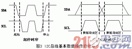
Careful observation of the basic data operation sequence of Figure 3 [1] can be found: First, the I2C bus is in a high state when there is no data transmission; Second, the SDA pin is the input and output of the data, its state changes most Complex, controlling it requires frequent use of P6IN, P6OUT, P6DIR three registers. R1 and R2 in Figure 2 are pull-up resistors whose resistance is determined by the electrical characteristics of the selected I2C bus device. In this paper, these two resistors not only play the role of pulling up, but also help solve the first problem. When P6.6 and P6.7 are in the receiving state, the pull-up resistor can pull the level of this point to VCC, thus ensuring a stable high level when the bus is idle. Continuing the above ideas, it can be found that when the corresponding bit of the direction register is an input, it is equivalent to sending a logic "1" to the I2C slave. So how do you send a logical "0"? The corresponding direction control bit is set to the output, and then the corresponding position of the output register is “0â€. Further, if the output register is set to "0", only two changes in the direction register can be controlled to transmit two logic levels. Thus, only the direction register needs to be controlled when transmitting data. For SDA, which requires frequent switching of input and output states, this method can reduce the amount of code by about 15% and make the program clearer. This finds a good solution for the second problem. [b]3 Implementation of I2C bus control timing The above describes the most basic operation timing of the I2C bus. The various operations in the I2C bus are done by a combination of these basic operations. Since the types, functions, and structures of the I2C bus devices are different, the specific control timing of each device is different. Figure 4 shows the AT2402 read specified byte data control timing. It can be seen from the figure that the basic operations of starting, sending bytes, processing responses, receiving bytes, and stopping are used in a read operation. The code in the appendix implements this timing. There are other control timings for the AT2402, such as byte write timing, data page read timing, address read timing, etc. [1]. The code in the appendix is ​​written as a subroutine for the basic operations. For different function timings, it can be implemented by calling a subroutine.

The LM92 is a high precision temperature sensor that is also controlled by the I2C bus. Figure 5 is a timing diagram of the device reading temperature data. Because its function and structure are very different from the AT2402, the control timing of the two is not the same. As shown in Figure 4 and Figure 5, although the read operation is implemented, the timing of the two is very different, and the control timing of the LM92 is obviously much more complicated. However, careful analysis shows that these timings are also implemented by a combination of basic operations. In this way, the basic operation subroutine required by the LM92 can be improved on the basis of the above method, and then the subroutine can be arranged to realize various control of the LM92 according to the timing requirement.

In summary, to achieve the control timing of the I2C bus, it is necessary to carefully analyze the timing requirements and characteristics of various devices, construct all the basic operations, and arrange the basic operations according to the timing requirements. [b]4 Conclusion Applying the above design method and circuit, the interface between MSP430 and I2C bus device is realized, and AT2402 and LM92 are well controlled, which achieves the expected goal. Practice has proved that this method is very effective for implementing I2C bus device control, and the program code compiled by this method is small in quantity and high in execution efficiency. This method provides a feasible solution for the MSP430 and I2C bus interface.
The anti-glare technology used in the Matte Protective Film can reduce glare to eliminate eye fatigue, and make it easier to watch under direct light, which is more friendly to your eyes.
In order to let you enjoy it for a long time, the Frosted Screen Protector uses durable military-grade TPU material, which has strong durability and scratch resistance. It protects the screen from unnecessary scratches.
It has good anti-fingerprint ability, sweat will not remain on the screen surface, and it is easy to clean without affecting touch sensitivity or response speed.
The adhesive layer ensures that you stick the Protective Film in a stress-free manner and maintain a strong adhesion without leaving any sticky residue.
If you want to know more about Matte Screen Protector products, please click the product details to view the parameters, models, pictures, prices and other information about Matte Screen Protector.
Whether you are a group or an individual, we will try our best to provide you with accurate and comprehensive information about the Matte Screen Protector!
Matte Screen Protector, Frosted Screen Protector, Matt Screen Protector, Matte Hydrogel Film, Matt Protective Film, Anti-Glare Screen Protector
Shenzhen Jianjiantong Technology Co., Ltd. , https://www.jjthydrogelprotector.com