Several commonly used embedded board communication interfaces
With the advent of the era of communication and computer integration, digitalization, broadband and intelligence have become the direction of future communication development. Human society has put forward higher and higher requirements for telecommunication services from quality to service types, and access networks as telecommunications. An important part of the network, connecting local switches and users, is the capillary and bottleneck of the entire telecommunications network, and the key to digitalization, broadband and business integration. The embedded system is a dedicated computer system based on application-centric hardware design and application-oriented software product development. It is widely used in manufacturing industry, process control, communication, instrumentation, instrumentation, automotive, marine, aerospace, aerospace, military equipment. , consumer products and other fields.
In an embedded system, an on-board communication interface refers to a communication path or bus used to interconnect various integrated circuits with other peripheral devices. The commonly used on-board communication interface will be explained one by one below.
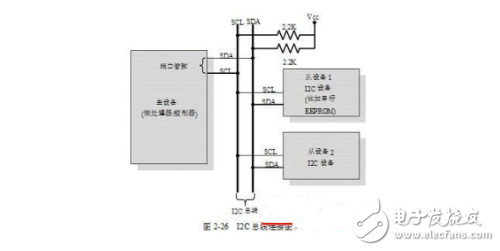
I2C busThe I2C bus is a synchronous, bidirectional, half-duplex, two-wire serial interface bus. Here, the meaning of half-duplex means that at any given moment, only one direction is communicable. The I2C bus was first developed by Philips Semiconductors in the 1980s. The original design goal of I2C was to provide an easy way to connect the microprocessor/microcontroller system to the peripheral chips of the TV. The I2C bus consists of two buses: a serial clock line SCL and a serial data line SDA. The SCL line is responsible for generating synchronous clock pulses, and the SDA line is responsible for transferring serial data between devices. The I2C bus is a shared bus system, so multiple I2C devices can be connected to the system. A device connected to the I2C bus can be used as both a master device and a slave device. The master device is responsible for controlling the communication, by initializing/terminating the data transfer, to send the data and generate the required synchronous clock pulses. The slave device is waiting for a command from the master device and responds to the command receipt. Both the master device and the slave device can function as a transmitting device or a receiving device. Whether the master device is acting as a transmitting device or a receiving device, the synchronous clock signal can only be generated by the master device. On the same bus, I2C supports the simultaneous presence of multiple master devices. Figure 2-26 shows the connection between the master and slave on the I2C bus.

An I2C bus interface can be constructed based on an input buffer and an open-drain transistor (or an open-collector transistor). When the bus is in an idle state, the open-drain transistor (or open-collector transistor) is left floating and the output conductors (SDA and SCL) are high impedance. In order for the bus to work properly, the pull-up resistor should be used to pull both buses up to the supply voltage (+5V for TTL series devices and +3.3V for CMOS series devices). Pull-up resistors typically have a value of 2.2K. When a pull-up resistor is used, the output conductor on the bus is in an idle state, corresponding to a high level.
The address of the I2C device can be assigned by connecting the device address line hardware to the desired logic level. In embedded devices, when designing embedded hardware, you need to assign addresses to various I2C devices and complete hardware connections. The working sequence of the system communicating with the I2C slave device is as follows:
(1) The master device pulls the clock line (SCL) on the bus high.
(2) When the SCL line is in the high logic (this is the start condition for data transfer), the master device pulls the data line (SDA) low.
(3) The master device transmits the slave device address (with 7-bit or 10-bit width) to the communication destination address through the SDA line. The slave generates a clock pulse on the SCL line for simultaneous bit reception. It should be noted that the system always transmits the MSB (most significant bit) of the data first. The data in the bus is active while the clock signal is high.
(4) The master device sends a read or write bit as required (a bit value equal to 1 means a read operation and a bit value equal to 0 means a write operation).
(5) The master waits for the slave to issue an acknowledgment bit. At the same time as the read/write operation command is sent, the address of the slave device is also sent to the bus. For slave devices connected to the bus, the received address is compared to the assigned address.
(6) If the slave device receives an instruction from the device and the address is correct, the slave device sends an acknowledgment bit (value 1) via the SDA line.
(7) After receiving the acknowledgment bit, the master device sends 8-bit data to the slave device via the SDA line if the operation command is to write data to the device. If the operation command is to read data from the device, the slave device will send the data to the master device via the SDA line.
(8) For the write operation, after the end of the byte transfer, the master waits for the slave to transmit an acknowledgment bit; for the read operation, after the end of the byte transfer, the master transmits an acknowledgment bit to the slave.
(9) When the clock line SCL is at a logic high level (indicating stop), the master device can terminate the data transfer by pulling the SDA line high.
The I2C bus supports three different data rates: standard mode (data rate is 100kb/s, ie 100kbps), fast mode (data rate is 400kb/s, ie 400kbps), high speed mode (data rate is 3.4Mb/s, ie 3.4Mbps). The first generation of I2C devices designed to support data rates of only 100 kbps, and next-generation I2C devices can operate at data rates up to 3.4 Mbps.
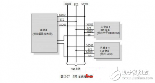
2. SPI busThe SPI bus is a synchronous, bidirectional, full-duplex 4-wire serial interface bus that was first proposed by Motorola. The SPI is a system consisting of "single master + multiple slaves". It should be noted that in the system, as long as only one master device is active at any time, there may be multiple SPI master devices. In order to achieve communication, SPI has four signal lines, which are:
(1) Master Out Slave In (MOSI): A signal line that transmits data from the master device to the slave device, also called slave input (Slave Input/Slave Data In, SI/SDI).
(2) Master In Slave Out (MISO): A signal line that transmits data from the slave device to the master device, also known as slave output (Slave Output/Slave Data Out, SO/SDO).
(3) Serial Clock (SCLK): A signal line that transmits a clock signal.
(4) Slave Select (SS): Used to select the signal line of the slave device, active low.
Figure 2-27 shows the connection between the master and slave on the SPI bus.

The master device is responsible for generating the clock signal and strobing the desired slave device by pulling the slave device select signal of the corresponding slave device low. When there is no strobe, the data output line MISO of all slave devices is suspended in a high impedance state.
Serial data transfer on the SPI bus is user configurable. The SPI device contains a specific register set that holds the required configuration. The control registers of the serial peripherals are used to store various configuration parameters such as master/slave selection of the device, selection of communication baud rate, clock signal control, and so on. The status register is used to save the status of various communication conditions to achieve the required data transmission and data reception.
The operation of the SPI is based on a shift register; for data transfer or data reception, the master and slave devices contain dedicated shift registers. The length of the shift register depends on the specific device and is usually an integer multiple of 8. During the transfer of data from the master to the slave, the data in the master shift register is shifted out of the MOSI pin and then input to the slave's shift register via the slave's MOSI pin. At the same time, the data shifted from the device shift register is input to the shift register of the master device through the MISO pin. That is, the master and slave shift registers form a circular buffer. For a particular type of device, the configuration register (for example, for the 68HC12 controller from Motorola, the LSBF bit of the SPI control register needs to be configured) determines whether the first transmitted data bit is the highest or lowest bit.
Compared with the I2C bus, the SPI bus is more suitable for data stream transmission. The downside of SPI is that SPI does not support data validation mechanisms.
3. UARTUART-based data transfer is an asynchronous form of serial data transfer. UART-based serial data transmission does not require the use of a clock signal to synchronize the transmitting and receiving ends of the transmission, but rather a predefined configuration between the transmitting device and the receiving device. For both the transmitting device and the receiving device, the serial communication configuration (baud rate, number of bits per unit word, parity, start and end bits, flow control) should be set to be identical. The start and end of the communication can be indicated by inserting a specific bit sequence into the data stream. When transmitting a byte of data, it is necessary to add a start bit at the beginning of the bit stream and add an end bit at the end of the bit stream. The lowest bit of the data byte is immediately after the start bit.
The start bit is used to inform the receiving device that the data byte is about to reach the receiving end. Then, the receiving device selects its data receiving line according to the set baud rate. If the baud rate is x bits/second, then the time slot available for each bit is 1/x second. The receiving device will accurately select the data receiving line at a position halfway of the bit available time slot. If the communication uses the parity function, the UART transmitting device adds a parity bit to the transmitted data stream (a value of 1 indicates that the transmitted bit stream contains an odd number of 1; a value of 0 indicates a transmitted bit stream) Contains an even number of 1). The UART receiving device calculates the parity result of the received data bits and compares it with the received parity bit. The UART receiving device discards the start bit, the end bit, and the parity bit in the received bit stream, and converts the received serial bit data into a word (for example, considering that 8 bits correspond to 1 byte, receiving Up to 8 bits, the first received data bit is the LSB, and the last received data bit is the MSB).
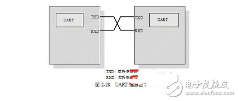
In order to achieve proper communication, the data transmission line of the transmitting device should be connected to the data receiving line of the receiving device. Figure 2-28 shows the connection diagram for the UART.

In addition to serial data transfer, the UART provides hardware handshake support for controlling serial data streams. Many semiconductor manufacturers have provided corresponding UART chips. The 8250 UART from NaTIonal Semiconductor is a standard-set UART for early design of IBM PCs.
Today, most microprocessors/controllers integrate UART functionality and provide built-in instruction support for serial data transmission and reception.
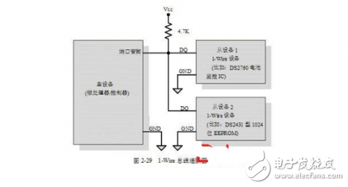
4. 1-Wire interfaceThe 1-Wire interface is an asynchronous half-duplex communication protocol developed by Maxim Dallas Semiconductor Corporation (home page), also known as the Dallas 1-Wire® protocol. Among them, according to the master-slave communication model, communication is realized using only a single signal line DQ. An important feature of the 1-Wire bus is that it allows energy to be transmitted on the signal line. The I2C slave uses an internal capacitor (typically 800 pF) on the signal line to drive the device. The 1-Wire interface supports the connection of a single master device and one or more slave devices on the bus. Figure 2-29 shows the connection between the master and slave on the 1-Wire bus.

Each 1-Wire device has the world's only identifiable 64-bit identification code information stored inside the device. For multiple slave devices connected to the 1-Wire bus, each individual device present on the bus can be addressed by interpreting the unique identification code. The identification code consists of three parts: an 8-bit class code, a 48-bit serial number, and an 8-bit CRC check result of the first 56-bit data. The specific process of communicating with 1-Wire slaves is as follows:
(1) The master sends a reset pulse to the 1-Wire bus.
(2) The slave device on the bus responds with an acknowledge pulse.
(3) The master sends a ROM command (network addressing command, the parameter is the 64-bit address of the device) to address the slave device that needs to initiate communication.
(4) The master sends a read/write command to read/write the slave's internal memory or registers.
(5) The master device reads data from the slave device or writes data to the slave device.
All communication on the 1-Wire bus is initiated by the master device. The minimum interval of communication is a time slot with a duration of 60 microseconds. The reset pulse occupies 8 time slots. At the beginning of the communication, the master pulls the 1-Wire bus low for eight time slots (480 μs) to issue a reset pulse. If there is a slave on the bus and it is ready for communication, the slave will respond to the master with an acknowledge pulse; that is, the slave pulls the 1-Wire bus low for one slot. (ie 60 μs). In order to write a bit value of 1 on the 1-Wire bus, the bus master is required to pull the bus low for a duration of 1 to 15 μs and then release the bus for the remainder of the time slot. In order to write a bit value of 0 on the bus, the master needs to pull the bus low for at least 1 time slot (60 μs) and up to 2 time slots (120 μs). In order to read the bit value from the slave device, the master device needs to pull the bus low for 1~15 μs. In response to the read data request of the master device, if the slave device wants to transmit a bit value of 1, the slave device only needs to release the bus during the rest of the time slot; if the slave device wants to send a bit value of 0, then the slave device needs to The remaining time period of the time slot pulls the bus low.
Pc Material,Pc Plastic Material,Pc Clear Material,Pc Material Properties
WENZHOU TENGCAI ELECTRIC CO.,LTD , https://www.tengcaielectric.com