These days we have been designing our own Cyclone V SoC development board. Because we are splinters, we absolutely do not have technical support from manufacturers and agents, so we can only look for a variety of ready-made solutions.
In fact, the peripheral circuit design of Cyclone V SoC chip is not difficult, nothing more than DDR3, Gigabit Ethernet PHY, USB PHY, USB to serial port. But in addition to these functional circuits, the more important thing is the power circuit.
Taking the DE0-Nano-SoC as a reference, a total of 10 voltages of 5V, 9V, 3.3V, 1.1V, 1.2V, 1.5V, 1.8V, 2.5V, and DDR VTT and VREF are involved on one board. Scared personally.
I have always heard that power supply design is very important. When I see so many power supplies, I feel awkward. However, no matter how troublesome, the solution to the problem still needs to be solved.
Since the boards on the market for Cyclone V SoC are not really on the market, and the DE0-Nano-SoC is a board with the simplest functionality, it uses its power solution as a reference.
5V: This to say, as a power input for the entire board, using a 10W power supply
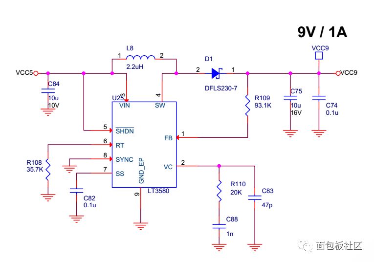
9V/1A: The 9V appears to be on the board for LTC's DAC add-in boards. A Boost boost circuit is used, irrespective of the core system.
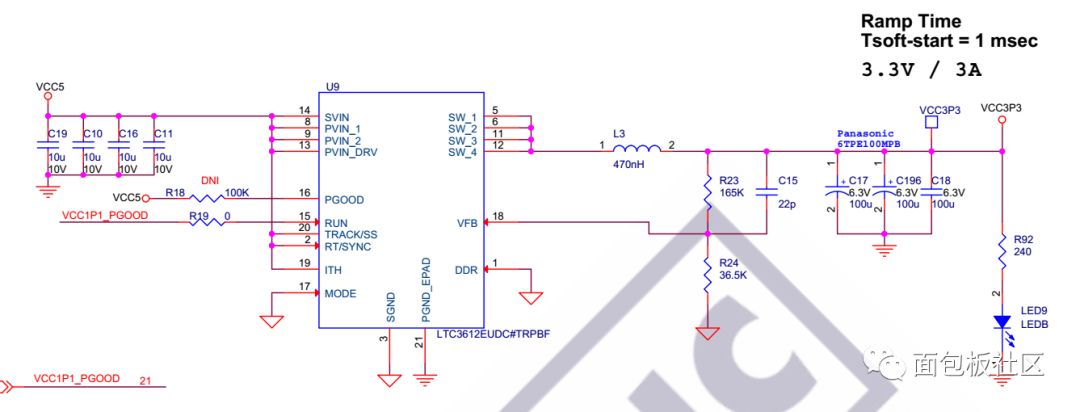
3.3V/3A: Almost every chip on the board needs 3.3V power supply, and some pin headers also need external power supply, so designing a 3A output has no doubt.
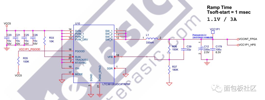
1.1V/3A: This power supply can be seen as being divided into two names at the time of output. One is VCCINT_FPGA and the other is VCC1P1_HPS. Since the FPGA core and HPS are to be powered at the same time, the design of the 3A current is not to blame. Only in fact there should be room for compression, but it is not necessary.
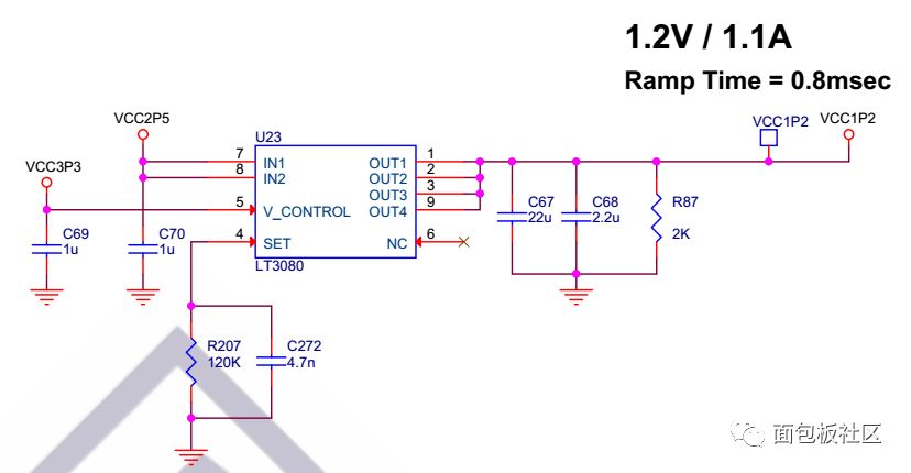
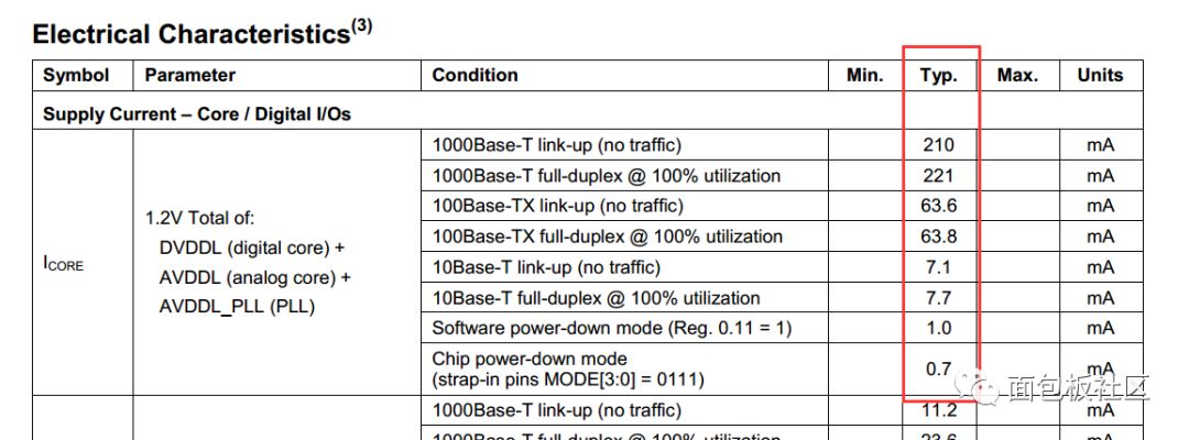
1.2V/1.1A: This is searched in the schematic diagram. It is only used for the core power supply of the Ethernet PHY chip. According to the description of the Ethernet chip manual, the typical operating current of the core power supply for Ethernet is shown in the following table. It can be seen that Gigabit full-duplex is only 221mA at 100% utilization rate, so personally think that the 1.2V/1.1A power supply design in this place is too wasteful, and the general Ethernet PHY chip comes with LDO control. Foot, using an AO3415 MOS tube will be self-sufficient. Therefore, this 1.2V/1.1A design cost is not high.
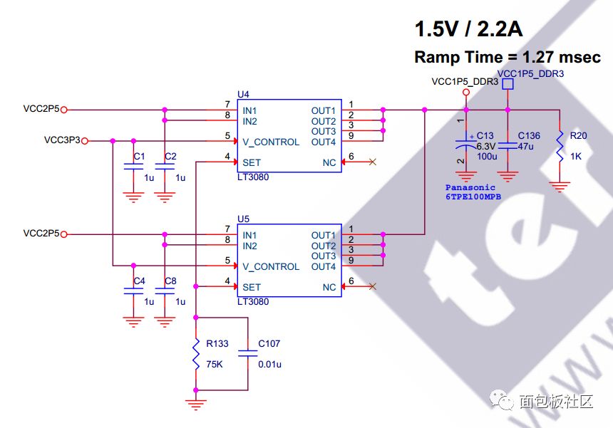
1.5V/2.2A: Really rich, using two 1.1A LDOs in parallel to get 2.2A output. This power supply is used to power the DDR3 chip. Since all of them have reached the current output of 2.2A, why do we have to use two LDOs in parallel instead of DCDC? Can DDR3 not be powered by DCDC? Or is it just for the sake of brushing? In addition, I would also like to know that the power consumption of two DDR3s is about the same. Is it necessary to use 2.2A current?
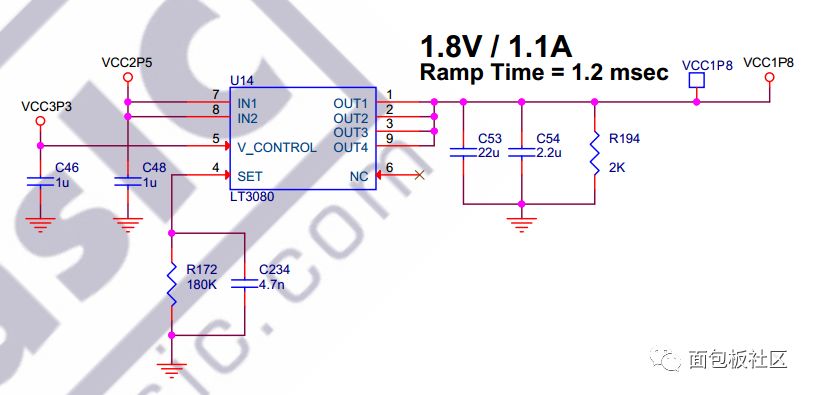
1.8V/1.1A: Looked on the schematic, this power supply has two main roles, one is to power the PLL chip, output multiple clocks for the FPGA and HPS clock, the other is for the onboard USB Blaster II The core chip of the downloader EPM570 type CPLD is used as the core power supply. Therefore, it has nothing to do with the Cyclone V SOC chip.
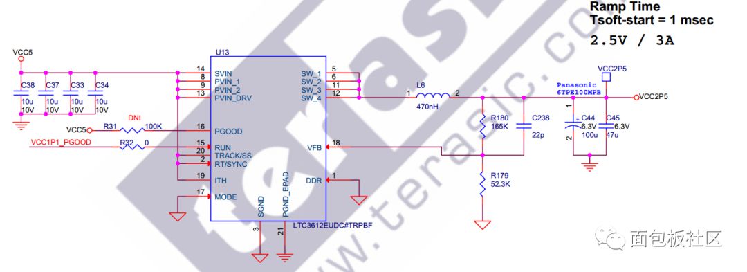
2.5V/3A: In the end, it was the 2.5V/3A that I was deeply puzzled by. At the beginning, I was always looking for the place where the 2.5V power was supplied. After checking it, I found that it was basically all connected to the pins of the SoC FPGA. I don't think so.
An FPGA chip, to do a 2.5V/3A power supply, the kernel is only 3A ah. The design schematics were stuck here long ago, and they have been puzzled. Even the fear of the power supply circuit design of the Cyclone V SOC chip has been dared to face them. Thigh, suddenly realized.
This 1.2V/1.1A, 1.8V/1.1A, 1.5V/2.2A power supply on the original board is used as input. Affection is to reduce power dissipation. Therefore, this 2.5V/3A power supply is mainly designed not for the chip but for other LDO power supplies. Initially calculated the following:
All other power supply circuits using 2.5V as input have a design power of 1.2*1.1+1.8*1.1+1.5*2.2 = 1.32+1.98+3.3=6.6W, while the 2.5V/3A design power is 7.5W, meaning only 0.9W is left to the SOC chip, the current down conversion is 360mA, which, this, this is solved with a common LDO. At this point, it finally figured out.
Intercome speaker:
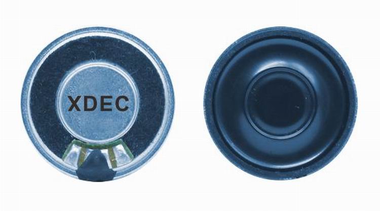
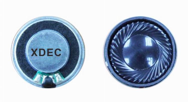
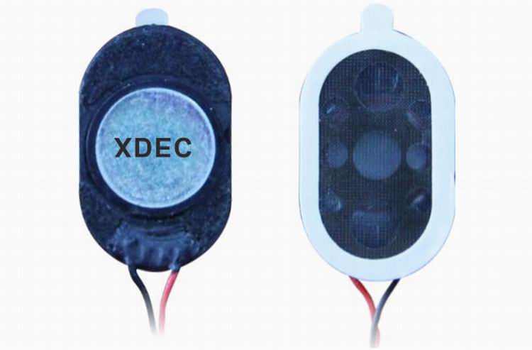
Intercome speaker is a kind of micro speaker unit which uses a diaphragm made of Mylar material. Mylar speakers are of ultrathin design and lightweight and clear voice. It is widely used in building security industry (e.g. intercom, video door phone, intelligent door control..)
There are two types of Mylar speakers from the shapes:
1) Round shapes, we have products from 10mm to 57mm in diameter.
2) Oblong shape, we have products in sizes of 1510/1712/1813-..
FAQ
Q1. What is the MOQ?
XDEC: 2000pcs for one model.
Q2. What is the delivery lead time?
XDEC: 15 days for normal orders, 10 days for urgent orders.
Q3. What are the payment methods?
XDEC: T/T, PayPal, Western Union, Money Gram.
Q4. Can you offer samples for testing?
XDEC: Yes, we offer free samples.
Q5. How soon can you send samples?
XDEC: We can send samples in 3-5 days.
Intercom Speaker,Handheld Intercom Speaker,Window Intercom Speaker,Building Intercom Speaker
Shenzhen Xuanda Electronics Co., Ltd. , https://www.xdecspeaker.com