bandwidth
Studying the modulation characteristics of light-emitting diode (LED) devices and the luminescence characteristics under high-speed modulation conditions is one of the key issues to improve the performance of new visible light communication systems. The improvement of modulation characteristics of LED devices can significantly expand the application range of visible light communication systems. Based on the FM characteristics of LED devices, by analyzing the structure of light-emitting devices and packages and other key optoelectronic properties, suggestions are made to improve the response rate of LED devices and improve the modulation bandwidth of LEDs by reducing RC time and carrier spontaneous emission lifetime.
1 LED device modulation bandwidth and its testing
Bandwidth generally refers to the bandwidth occupied by the signal. When describing a channel, bandwidth refers to the maximum bandwidth that can effectively pass the channel signal. The modulation bandwidth of a light-emitting diode (LED) is the bandwidth of the device that can carry the maximum signal when the modulated signal is loaded. Generally, the AC power output of the LED is reduced to a half of a low-frequency reference frequency (eg, -3 dB). The frequency is determined by the modulation bandwidth of the LED. The modulation bandwidth of LED is a decisive factor for the channel capacity and transmission rate of visible light communication systems, and is affected by many factors such as the actual modulation depth and volt-ampere characteristics of the device.
The test of the modulation bandwidth of an LED device is usually performed by loading an analog signal (such as a sinusoidal signal) on a device under direct current operation and measuring a curve of the optical power signal as a function of frequency to determine the bandwidth.
Figure 1 shows a device modulation characteristic test system [1-3]. It mainly includes the signal transmitting end and the receiving end. At the transmitting end, the signal from the signal generator is amplified by the power amplifier to increase its modulation depth; subsequently, the signal is applied to the DC bias of the driving LED so that the LED emits a modulated optical signal; at the receiving end, the photodetector emits light The signal is converted into an electrical signal, filtered and amplified, and output to the oscilloscope.
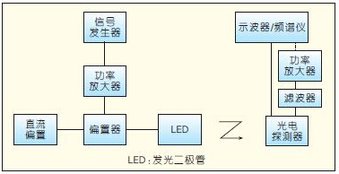
Figure 1 device modulation characteristics test system composition
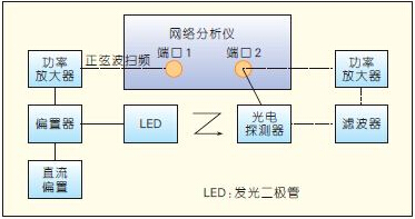
Figure 2 device modulation characteristics test system composition
Figure 2 is another device modulation characteristic test system [4-5]. At the heart of the system is a network analyzer that integrates signal generation, detection, and processing functions to enable higher frequency testing. Measuring the LED modulation bandwidth, mainly focusing on the S21 parameter of the network analyzer, that is, the input power of port 2 of the network analyzer/the output power of port 1.
bandwidth
2 Influencing factors and improvement methods
In general, the factors affecting the modulation characteristics of LEDs mainly depend on the following two aspects [6]: RC time and carrier spontaneous emission lifetime. The active area of ​​the LED is a multi-quantum well structure with charge-limiting function. The rise and fall time in the response process is called RC time, which is mainly affected by the junction capacitance and has a delay effect on the signal. The carrier in the active region of the device Spontaneous radiation lifetime directly affects the time from carrier recombination to photon escape from the device.
2.1 Reduce RC time
Figure 3 shows the small signal equivalent circuit of the LED [7]. This small signal equivalent circuit is actually similar to the equivalent circuit of a laser at a threshold voltage. Since the laser device operates in a spontaneous emission state at a threshold voltage and the stimulated emission process has not yet started, the LED also uses the equivalent circuit [8-11].
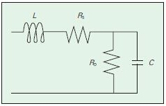
Figure 3 LED small signal equivalent circuit
Where C is the junction capacitance, RD is the junction resistance, RS is the equivalent series resistance, and L is the parasitic inductance caused by the lead. The researchers can obtain these corresponding key parameters through experimental measurements and theoretical fitting [7-8]. The capacitance and geometric capacitance obtained here are an order of magnitude, and the resistance is similar to the geometric resistance. Therefore, the size of the device can effectively adjust the equivalent circuit parameters and thus increase the device bandwidth.
It is a relatively straightforward way to reduce the RC time by the size of the device to improve the LED modulation bandwidth. The effect of size on LED bandwidth was studied by designing a set of LED devices of different sizes (junction area, p-GaN and junction contact area) [4]. A device with a larger active area has a smaller modulation bandwidth at the same current density. The reason is mainly because the equivalent junction capacitance is larger, and the effect of the increase in capacitance on the bandwidth is more significant than the effect of the resistance reduction. This result is consistent with the results of J.-W. Shi et al. [6] of Taiwan's successful university. Figure 4 shows the frequency response curves of experimental devices A and B at different drive currents. A device p-GaN has a larger contact area with the junction.
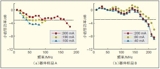
Figure 4 Frequency response curves of two different sized devices at multiple drive currents
Figure 4 also reflects the effect of different currents on the LED bandwidth. At high currents, the carrier concentration increases, resulting in a composite enhancement in the multiple quantum wells and a reduced carrier lifetime of the carriers.
Chien-Lan Liao et al. [12] of Tsinghua University in Taiwan used a gallium-doped (Ga) zinc oxide (ZnO) film GZO to effectively reduce the junction capacitance. Figure 5 shows a schematic diagram of a blue LED structure with a current confinement layer. Since the p-type GaN layer is carved out of the mesa and the electrode is formed on the p-type, the effective capacitance can be reduced. Moreover, the electrode adopts a ring structure, and the GZO film with large lateral resistance is used to realize current limiting, so that the current is mainly transmitted in the vertical direction, that is, GZO realizes the opposite function to indium tin oxide (ITO), and suppresses current expansion. Therefore, the actual junction capacitance will become smaller, thereby achieving an increase in the LED modulation bandwidth. With this ring electrode design, the device has a 3 dB bandwidth of 225 MHz.
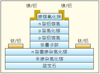
Figure 5 Epitaxial wafer structure using GZO as current limiting layer
Xu Jinyi and others from Taiwan's Central University [13] also effectively increased the LED modulation rate by means of a series connection, and the starting point is also based on the optimization of the RC time. If N identical LEDs are connected in series, the resistance value will increase linearly by R total = N · R, while the capacitance value decreases linearly by C total = C / N. This way, although the RC time has not changed. However, in general, the device needs to be externally connected, so the actual RC is (N·R+R0)·C/N, so it is smaller than the RC (RC+N·R0C) of a single LED of the same area, so that the modulation bandwidth can be effectively improved.
bandwidth
2.2 Reduce the spontaneous emission life of carriers
Visible light (VLC) communication systems generally operate over a wide current range, so it is also necessary to study the frequency response at different currents. Figure 6 shows the device frequency response curves at different currents. The larger the applied drive current, the greater the 3 dB bandwidth of the electro-optic conversion (EO) [12-15]. As can be seen from Figure 6, the modulation frequency at 120 mA is approximately twice that at 40 mA. Mainly because the exciton recombination probability is proportional to the injected carrier density [6]. At high currents, the injected carrier concentration increases, so the exciton recombination probability increases, the radiative recombination carrier lifetime decreases, and the EO responds quickly.
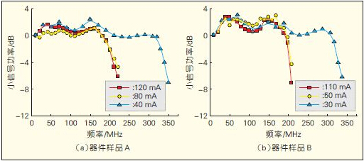
Figure 6 Effect of different currents on the modulation frequency of the device
There are many factors affecting the spontaneous emission lifetime of carriers. Generally speaking, the external factors are mainly the concentration of injected carriers; while the internal factors are mainly due to the structure of the device itself and other composite channels.
M. Feng et al. [16] of the University of Illinois at Urbana-Champaign increased the modulation rate by an order of magnitude to the gigahertz level through an LED similar to a heterojunction bipolar light-emitting transistor (HBLET). HBLET is a 3-port light-emitting device (an electrical input, an electrical output, and a light output). The quantum well active region is incorporated into the base region, which improves the electrical and optical properties, while the high-speed LED structure and HBLET is similar. At 60 mA drive current, the device's EO modulation frequency is as high as 7 GHz, but the power is small, only about 13.8 μW. Figure 7 is a schematic diagram of the structure of the device (npn structure). It can be seen that the emitter is connected to a negative voltage, and the base and the collector (this is also called the drain Drain) are connected to the positive electrode, so that the emitter junction is positively biased and the collector junction is reverse biased. Since the base and drain have the same potential, there is no charge distribution accumulation at the base-drain boundary. Under AC drive, a dynamic charge distribution of the emitter and drain is established in the base region. Therefore, the lifetime of the spontaneous carrier recombination of the excess carrier in the base region is greater than the transmission time from the emitter to the drain, so that the carrier has not yet been recombined, and the built-in reverse electric field is swept to the drain, leaving only the fast. The carrier composite illuminates, thereby increasing the modulation speed.
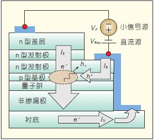
Figure 7 High-speed Tilted-charge LED structure
Figure 8 shows the frequency test results for EO. The modulation frequency is very high, and as the current increases, the modulation speed increases, reaching 7 GHz at 60 mA. This result is the same as that of a plastic fiber optic light emitting diode (POF-LED). However, there is a big problem that the power of the device is very small. Under the forward bias of 3 V, the drive current reaches 60 mA, and the corresponding optical power is only 15 μW, which is totally unsuitable for lighting LEDs. Provides an idea to improve the bandwidth of high power LEDs.
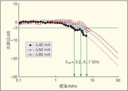
Figure 8 Frequency characteristics at different drive currents IE (charge tilt distribution LED (25 ° C))
The carrier recombination mechanism in the material includes radiation composite and non-radiative recombination. Surface plasmon coupling is the third energy transfer channel in addition to the first two, which can also affect the radiated composite carrier lifetime and increase the LED modulation bandwidth.
Koichi Okamoto et al. [17] of the California Institute of Technology first used surface plasmons on LEDs to get an increase in light output. Document [18] provides a new technical approach to carrier-combined emission photons. As shown in Figure 9, the energy conversion of carrier recombination has multiple pathways, including radiative recombination, non-radiative recombination, and quantum well-surface plasmon (QW-SP) coupling. Non-radiative recombination can not produce photons, and energy is finally dissipated in the form of heat; radiation recombination can generate photons, and some of the generated photons can overflow the device, and the number of escaped photons can be reflected by the external quantum efficiency. The black arrows in Figure 9 indicate possible forms of QW-SP coupling. After the carrier recombination, the energy is not directly converted into photons, but is coupled to a surface plasmon (SP) that is relatively close (about 30 nm), and then emits energy out of the LED in the form of radiation. This process is much faster than the radiant composite energy conversion. At 490 nm, the difference is significantly reduced. This is because the QW-SP coupling wavelength is in blue light, so the position of the long wavelength, the energy coupling is weakened, and the difference is reduced.
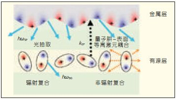
Fig. 9 QW coupling with surface SP during electron hole recombination
The bandwidth of the LED device can also be improved by the Al component regulation [5] and the delta doping technique [19]. Al component regulation, the principle is mainly to change the energy band structure, achieve effective injection of holes, regulate the polarization electric field, thereby improving the modulation bandwidth, the bandwidth is increased from 23.5 MHz to 25.5 MHz under 300 mA working current; delta doping The technology realizes a large amount of carrier injection, thereby reducing the carrier lifetime and achieving an increase in modulation bandwidth at the same current density. Figure 10 shows an eye diagram of the device after delta doping.
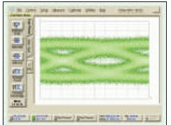
Figure 10 Delta doped LED device at 40 mA 260 Mb/s eye diagram
3 Conclusion
With the improvement of light efficiency and cost reduction, LED has been widely used in information display and various functional lighting. The visible light communication utilizes the characteristics of high luminous efficiency and high response rate of the LED compared to the conventional light source, and realizes the wireless data transmission function while illuminating. Conventional white LED devices typically have a modulation bandwidth of only 3 to 5 MHz, which limits the further improvement of the bandwidth of the visible light communication system. By appropriately adjusting the structure of the material and the chip, optimizing the process parameters of the device, introducing new radiation complexes such as surface plasmons. Mechanisms and other methods can effectively improve the modulation bandwidth of LED devices and further expand the application range of visible light communication systems.
The multimedia wiring harness apply to Audio,Video,Radio, LVDs,Flat RCA,USB.
Yacenter has experienced QC to check the products in each process, from developing samples to bulk, to make sure the best quality of goods. Timely communication with customers is so important during our cooperation.
If you can't find the exact product you need in the pictures,please don't go away.Just contact me freely or send your sample and drawing to us.We will reply you as soon as possible.
Electric Fan Wiring Kit,Socket Fan Wiring Harness,Custom Pc Wiring Harness,Multimedia Wiring Harness
Dongguan YAC Electric Co,. LTD. , https://www.yacentercn.com