Wiring means the arrangement of the wire connections between components. First wire the wires and pass the wires through the holes where the pins are electrically connected. This allows the components to be connected while soldering the components.
Wiring skillsWhen making the experimental board of the single-chip microcomputer, the 1-pin of the soldering digital tube should be led out by the wire and connected to the I/O port. The spacing between the pins is very small, which is a big challenge for beginners. In the first welding, the 4-digit digital tube was first soldered to the board, and then the wires were soldered on 12 pins. This is very troublesome, not only the soldering wire on the pin is troublesome, but also when wiring It is also very troublesome, because the a~h of the digital tube is not arranged in order. The lines are easy to cross. After thinking about it, you can wire and solder the components first, which is very simple and very fast.
Wiring specific operationFirst wire the wires and pass the wires through the holes where the pins are electrically connected. This allows the components to be connected while soldering the components. For more pins, small pin spacing, and more intensive electronic components, such as digital tubes, then you must first wire the wires before soldering the components, otherwise it is cumbersome to solder the wires on the densely packed pins. This type of component must first pass the wire through the hole where the pin is located on the universal board (bread plate), and fix the wire on the board with spot solder elsewhere. Here, you can choose a thin copper wire for the wire, and directly find a wire made of thin copper wire. Stripping the insulation is a ready-made thin copper wire. Insert the electronic components and solder them to the pins.
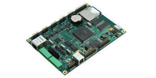
â—†High-frequency digital circuit is thinner and shorter.
â—† High current signal, high voltage signal and small signal should be separated from each other (the isolation distance is related to the withstand voltage to be withstand. Usually, the distance is 2mm on the board at 2KV, and the ratio is increased above this. For example, if you want to withstand the withstand voltage test of 3KV, the distance between the high and low voltage lines should be more than 3.5mm. In many cases, to avoid creepage, the slot between the high and low voltage on the printed circuit board is also required.)
â—†When two panels are wired, the conductors on both sides should be perpendicular, oblique, or curved, avoiding parallel to each other to reduce parasitic coupling. The printed conductors for the input and output of the circuit should be parallel to the rabbits. In order to avoid feedback, it is best to add a grounding wire between these wires.
â—†The corner of the line should be as large as 90 degrees, the corner below 90 degrees should be eliminated, and the corner of 90 degrees should be used as little as possible.
Same as the address line or the data line, the difference in the length of the trace should not be too large, otherwise the short-term part should be compensated for the bend line.
â—†The trace should be as far as possible on the soldering surface, especially the PCB of the through hole process.
â—†Use fewer vias and jumpers as much as possible
â—†The single-panel pad must be large, the line connecting the pad must be thick, and the teardrop can be placed on the teardrop. The quality of the general single-panel manufacturer will not be very good, otherwise there will be problems with soldering and RE-WORK.
â—†Large-area copper should be meshed to prevent bubbles from forming on the board during wave soldering and bending due to thermal stress. However, in special occasions, the flow direction and size of GND should be considered. It cannot be simply filled with copper foil. But need to go to the line
â—† Components and traces should not be placed too far on the side. Generally, the single panel is mostly a paper board. It is easy to break after being stressed. If it is connected at the edge or placed on the component, it will be affected.
â—† must consider the convenience of production, commissioning and maintenance
It is very important for the analog circuit to deal with the problem. The noise generated on the ground is often inconvenient, but once it is generated, it will cause great trouble and should be satin. For the power amplifier circuit, very small ground noise will have a significant impact on the sound quality due to the amplification of the latter stage; in the high-precision A/D conversion circuit, if there is a high-frequency component on the ground line, a certain temperature drift will occur, affecting The work of the amplifier. At this time, you can add the è—• capacitor at the 4 corners of the board, one foot and the ground connection on the board, and one foot to the mounting hole (connected by the screw and the case), so that this component can be taken care of, the amplifier and AD also It is stable.
In addition, the issue of electromagnetic compatibility is even more important in the current situation of people paying more attention to environmentally friendly products. Generally speaking, there are three sources of electromagnetic signals: signal source, radiation, and transmission line. The crystal oscillator is a common high-frequency signal source. The energy value of each harmonic of the crystal oscillator on the power spectrum will be significantly higher than the average value. It is feasible to control the amplitude of the signal, ground the crystal oscillator case, shield the interference signal, and use special filter circuits and devices.
Need to specify is the serpentine routing, because the application is different, its role is also different, in the computer's motherboard used in some clock signals, such as PCIClk, AGP-3lk, its role has two points: 1, impedance matching 2. Filter inductor.
For some important signals, such as HUBLink in the INTELHUB architecture, a total of 13 frequencies, up to 233MHZ, must be strictly equal in length to eliminate the hidden danger caused by time lag. At this time, serpentine routing is the only solution.
Generally speaking, the line spacing of the serpentine trace is >=2 times the line width; if it is in the ordinary PCB board, in addition to the function of the filter inductor, it can also be used as the inductor coil of the radio antenna and the like.
PCB wiring tips1, power, ground processing
In the PCB layout, the handling of the power and ground wires is very important. The noise interference generated by the power cables and ground wires should be minimized to ensure the quality of the products.
The wiring rules for the power and ground wires are as follows.
· Add a decoupling capacitor between the power supply and ground.
· Try to widen the power line and ground line width. It is better to make the ground line wider than the power line.
The PCB of the digital circuit can be formed into a loop by using a wide ground wire, that is, a ground net is used, and the ground of the analog circuit cannot be used in this way.
· Use a large area of ​​copper as the ground wire, connect the unused areas on the printed circuit board to the ground for grounding, or make a multi-layer board, each of which is occupied by a power supply and a ground.
Rule check
After the wiring design is completed, it is necessary to carefully check whether the wiring design meets the rules set by the designer, and also to confirm whether the established rules meet the requirements of the printed circuit board production process, and generally check the following aspects.
• Whether the distance between the wire and the wire, the wire and the component pad, the wire and the through hole, the component pad and the through hole, and the through hole and the through hole are reasonable, and whether the production requirement is satisfied.
• Is the width of the power and ground wires appropriate? Is there a tight coupling between the power supply and the ground (low wave impedance)? Is there a place in the PCB where the ground wire can be widened?
• Whether the best measures are taken for the critical signal line, such as the shortest length, the added protection line, the input line and the output line are clearly separated.
• Whether the analog circuit and the digital circuit part have separate ground lines.
• Whether the graphics (such as icons and markers) added to the PCB will cause a signal short circuit.
· Modify some ideal line shapes.
· Whether the process line is added on the PCB, whether the solder resist meets the requirements of the production process, whether the solder mask size is appropriate, and whether the character mark is pressed on the device pad.
• Whether the outer frame of the power ground layer in the multilayer board is reduced, such as a copper foil on the power supply ground layer, which is likely to cause a short circuit outside the exposed board.
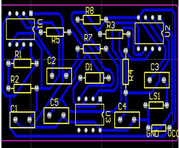
Pcb wiring effect
2. Co-processing of digital circuits and analog circuits
Many PCBs are no longer single-function circuits (digital or analog circuits), but rather a mixture of digital and analog circuits.
Therefore, it is necessary to consider the mutual interference between them when wiring, especially the noise interference on the ground. The frequency of the digital circuit is high, and the sensitivity of the analog circuit is strong. For the signal line, the high-frequency signal line is as far as possible away from the sensitive analog circuit device. For the ground line, the whole human PCB has only one node to the outside, so The number of processing and the common ground must be handled inside the PCB, and the digital ground and the analog ground inside the board are actually separated from each other, but only at the interface where the PCB is connected to the outside (such as a plug). The digital ground is slightly shorted to the analog ground. Please note that there is only one connection point. There is also no common ground on the PCB, which is determined by the system design.
3. The signal line is laid on the electrical (ground) layer.
When wiring the multi-layer printed circuit board, since there are not many lines left in the signal line layer, the additional layer processing is wasteful, and a certain amount of work is added to the production, and the cost is also increased accordingly. To solve this contradiction, consider wiring on the electrical (ground) layer. The first should consider the power layer, followed by the ground. This is better to preserve the integrity of the formation.
1. How to enter this wiring rule option of the PCB
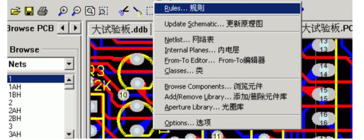
2. Setting of electrical safety distance

3. Wire width setting
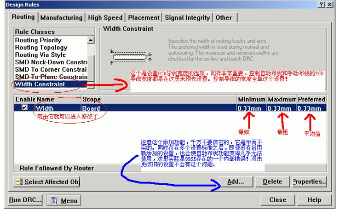
4. Learn to set up layers to make single-panel and multi-layer boards, not just double-panel
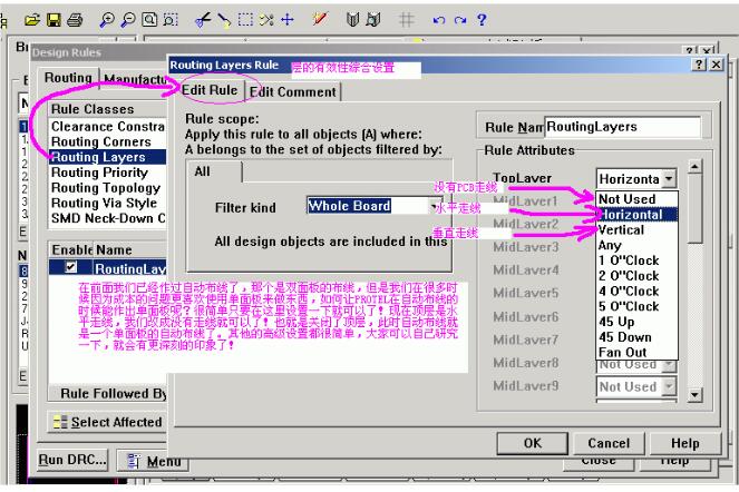
5. Setting of the corner section of the wiring middle line
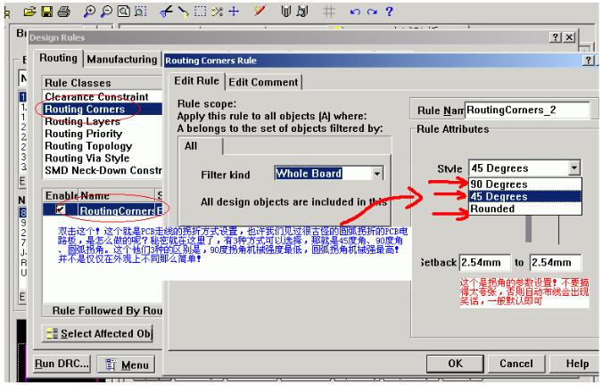
6. Selection of wiring type
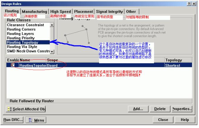
7. Some other settings
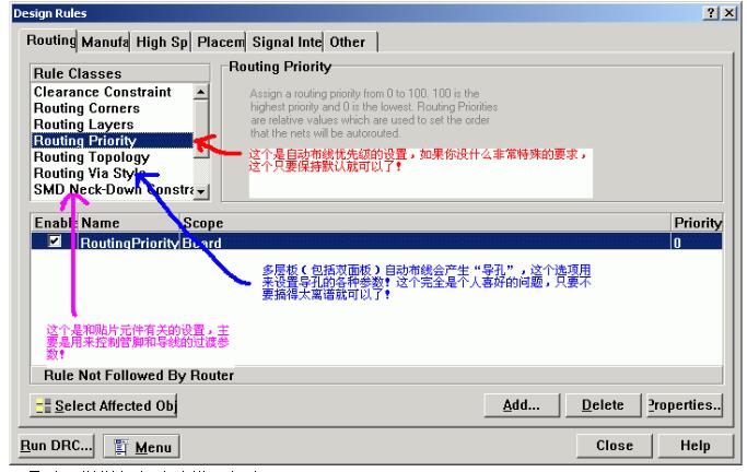
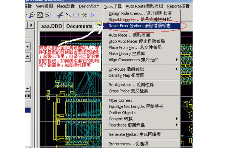
8. Finally learn how to clear the wrong sign
In conclusion, reading is a hobby that brings me immense pleasure and enriches my life in numerous ways. It stimulates my mind, enhances my creativity, and broadens my horizons. I am grateful for the world of books and the endless possibilities they offer.

In conclusion, reading is
2222Bossgoo(China)Tecgnology.
(Bossgoo(China)Tecgnology) , https://www.cn-gangdao.com