Moore's Law has been going on for more than half a century, from 90nm to 65nm, 45nm to 32nm... However, in the actual process manufacturing perspective, Moore's Law has been tested and questioned again and again, such as the 45nm HKMG process developed by Intel in 2007 and the 22nm finFET structure developed by Intel in 2011. The bigger problem is that after 28nm, the cost reduction of the law has begun to be questioned, coupled with the high cost of research and development, many IDM plants such as Motorola, NXP, Renasas, etc. turned to fab lite.
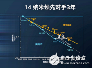
At Intel's sophisticated manufacturing day just held in September, Intel proved that Moore's Law is still valid, announced the launch of 10nm wafers, is developing 7nm, and developing 5nm and 3nm. Intel emphasized that the wafer process should be based on density, indicating that its 10nm is three years ahead of its competitors. In addition, Intel expands its foundry program, using 22FFL technology as a process technology for IoT mobile internet products, and working with ARM to strengthen its competitiveness in the Internet of Things.
Moore's Law is still valid 10nm wafers have been produced and developed 7nm5nm3nm.
As wafer fabrication processes continue to advance, each new process node becomes more difficult and costly. Just installing equipment into existing fabs costs nearly $10 billion, and fewer companies can afford the cost of moving Moore's Law.

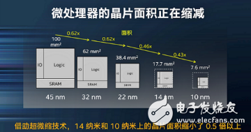
On Intel Manufacturing Day, Intel released 10nm wafers. By adopting hyper scaling, Intel's 10nm process technology has the world's densest transistors and the smallest metal pitch, enabling the industry's highest transistor density. Ultra-compact technology allows Intel to increase transistor density by 2.7x on 14nm and 10nm process nodes, reducing wafer area by more than 0.5x on 14nm and 10nm.
"Moore's Law is still valid," said Stacy Smith, executive vice president of Intel Corporation. "Transistor density has been increasing rapidly. Our new generation of transistor technology will bring a huge breakthrough. This is the driving force behind Moore's Law. We know The number of transistors in each node is doubled, and the 14- and 10-nanometer process technologies have all set a historical record, achieving higher transistor densities than the usual process. The normal manufacturing cost is rising, if the cost rises But the transistor shrinks. In fact, the cost per transistor is declining. It can be seen that the cost reduction of the last two nodes is higher than the historical trend."
Moore's Law will continue to move forward. Intel Senior Fellow and Intel Corporation's Director of Process Architecture and Integration, Ma Bo said: "In addition to the 10nm release and production, Intel is developing 7nm technology, 5nm and 3nm have been cutting-edge research, including: nanowire transistors, 3D stacking, EUV patterning, neuron technology, and the like.
The wafer process should be based on density and its leading edge of 14nm/10nm for 3 years.
With Moore's Law going to the extreme, the only companies that can follow up are Grotefonte, Samsung, TSMC and Intel. Among them, TSMC and Samsung have previously announced the promotion of the 10nm process. In response to the incitement of the process leader, Intel responded positively.
"16nm, 14nm, 10nm, 7nm, it looks like a horse. The problem is that these process node numbers have a real physical meaning, but now it is not the case," Stacy Smith said.
For the reason why the process node figures are meaningless, the semiconductor industry expert Mo Dakang pointed out the reasons behind it. He told reporters: "Because the previous definitions have been compared according to the length of the grid, it is technically difficult to find a suitable method to define."
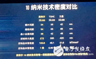
In this regard, Intel emphasizes the need to have an indicator to describe the performance of a certain process, showing the available transistor density for chip designers. Mabo said: "The advancement of the process technology should be based on the transistor density index. According to the transistor density index, Intel's 14nm can be compared with the 10nm of the friend, the latest 10nm lead friend for 3 years."


In this regard, Intel positively compared the relevant parameters of Samsung and TSMC in the same process node. I don't know what Samsung and TSMC will see when they see such a comparison chart.
"From 14nm, basically said each. There are two main factions: one is TSMC and Samsung's foundry lineup, and the other is Intel's CPU, because the memory has long since left the law to narrow the rules. Obviously take each need, Dress up as an advanced one. TSMC, Samsung is a pioneer, and Intel is different, Intel is IDM, there is an intrinsic demand for size, each silicon can have more chips. Measuring the advanced, can be derived from the annual R & D investment As a reference," Mo Dakang believes.
A solar Controller is an electronic device that controls the circulating pump in a solar hot water system to harvest as much heat as possible from the solar panels and protect the system from overheating.
Two kinds solar controller included:
2.MPPT Controller
MPPT stands for Maximum Power Point Tracking. MPPT is a technique to observe and regulates the energy going from Solar Panel to the batteries. Solar panels show changeable outputs according to weather conditions. MPPT charge control devices can match the solar panel voltage with Battery voltage to maximize the charge efficiency. In these systems, the full power of solar panels can be used by balancing between voltage and current according to the P = V x A equation. For example, the amount of current drawn from the panels reduced to protect the voltage when the weather is cloudy. When the weather is sunny, it is allowed to draw more current.
The main difference between PWM and MPPT charge control devices is that the MPPT devices are more efficient. MPPT charge control devices have 30 % more efficient in charge efficiency according to PWM type. Panel voltage and battery voltage should be matched in PWM systems. In MPPT systems, the panel series are allowed to have higher voltage than batteries. This means more flexibility for system growth.
Solar Charge Controller,Mppt Solar Charge Controller,Mppt Charge Controller,Mppt Solar Controller
NANTONG RONGCHANG IMPORT&EXPORT CO.,LTD , https://www.ergsolarcn.com